- 您現(xiàn)在的位置:買賣IC網(wǎng) > PDF目錄68456 > W3H128M72E-400SBI (WHITE ELECTRONIC DESIGNS CORP) 128M X 72 DDR DRAM, 1.35 ns, PBGA208 PDF資料下載
參數(shù)資料
| 型號: | W3H128M72E-400SBI |
| 廠商: | WHITE ELECTRONIC DESIGNS CORP |
| 元件分類: | DRAM |
| 英文描述: | 128M X 72 DDR DRAM, 1.35 ns, PBGA208 |
| 封裝: | 16 X 22 MM, 1 MM PITCH, PLASTIC, BGA-208 |
| 文件頁數(shù): | 17/32頁 |
| 文件大小: | 988K |
| 代理商: | W3H128M72E-400SBI |
第1頁第2頁第3頁第4頁第5頁第6頁第7頁第8頁第9頁第10頁第11頁第12頁第13頁第14頁第15頁第16頁當(dāng)前第17頁第18頁第19頁第20頁第21頁第22頁第23頁第24頁第25頁第26頁第27頁第28頁第29頁第30頁第31頁第32頁
W3H128M72E-XSBX
24
White Electronic Designs Corporation (602) 437-1520 www.whiteedc.com
White Electronic Designs
September 2009
Rev. 6
White Electronic Designs Corp. reserves the right to change products or specications without notice.
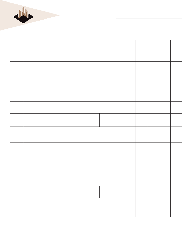
DDR2 ICC SPECIFICATIONS AND CONDITIONS
VCC = 1.8V ±0.1V; -55°C ≤ TA ≤ 125°C
Symbol
Proposed Conditions
667
CL6
533
CL5
400
CL4
Units
ICC0
Operating one bank active-precharge current;
tCK = tCK(ICC), tRC = tRC(ICC), tRAS = tRASmin(ICC); CKE is HIGH, CS# is HIGH between valid commands;
Address bus inputs are SWITCHING; Data bus inputs are SWITCHING
675
575
574
mA
ICC1
Operating one bank active-read-precharge current;
IOUT = 0mA; BL = 4, CL = CL(ICC), AL = 0; tCK = tCK(ICC), tRC = tRC (ICC), tRAS = tRASmin(ICC), tRCD =
tRCD(ICC); CKE is HIGH, CS# is HIGH between valid commands; Address bus inputs are SWITCHING;
Data pattern is same as IDAD6W
800
675
mA
ICC2P
Precharge power-down current;
All banks idle; tCK = tCK(ICC); CKE is LOW; Other control and address bus inputs are STABLE; Data
bus inputs are FLOATING
55
mA
ICC2Q
Precharge quiet standby current;
All banks idle; tCK = tCK(ICC); CKE is HIGH, CS# is HIGH; Other control and address bus inputs are
STABLE; Data bus inputs are FLOATING
325
225
200
mA
ICC2N
Precharge standby current;
All banks idle; tCK = tCK(ICC); CKE is HIGH, CS# is HIGH; Other control and address bus inputs are
SWITCHING; Data bus inputs are SWITCHING
350
300
250
mA
ICC3P
Active power-down current;
All banks open; tCK = tCK(ICC); CKE is LOW; Other control and
address bus inputs are STABLE; Data bus inputs are FLOATING
Fast PDN Exit MRS(12) = 0
200
175
150
mA
Slow PDN Exit MRS(12) = 1
50
mA
ICC3N
Active standby current;
All banks open; tCK = tCK(ICC), tRAS = tRASMAX(ICC), tRP = tRP(ICC); CKE is HIGH, CS# is HIGH between
valid commands; Other control and address bus inputs are SWITCHING; Data bus inputs are
SWITCHING
375
275
250
mA
ICC4W
Operating burst write current;
All banks open, Continuous burst writes; BL = 4, CL = CL(ICC), AL = 0; tCK = tCK(ICC), tRAS =
tRASMAX(ICC), tRP = tRP(ICC); CKE is HIGH, CS# is HIGH between valid commands; Address bus inputs
are SWITCHING; Data bus inputs are SWITCHING
1,250
950
800
mA
ICC4R
Operating burst read current;
All banks open, Continuous burst reads, IOUT = 0mA; BL = 4, CL = CL(ICC), AL = 0; tCK = tCK(ICC), tRAS =
tRASMAX(ICC), tRP = tRP(ICC); CKE is HIGH, CS# is HIGH between valid commands; Address bus inputs
are SWITCHING; Data pattern is same as IDAD6W
1,375
975
900
mA
ICC5
Burst auto refresh current;
tCK = tCK(ICC); Refresh command at every tRFC(ICC) interval; CKE is HIGH, CS# is HIGH between valid
commands; Other control and address bus inputs are SWITCHING; Data bus inputs are SWITCHING
1,400
1,300
1,250
mA
ICC6
Self refresh current;
CK and CK# at 0V; CKE 0.2V; Other control and address bus inputs
are FLOATING; Data bus inputs are FLOATING
Normal
45
mA
ICC7
Operating bank interleave read current;
All bank interleaving reads, IOUT = 0mA; BL = 4, CL = CL(ICC), AL = tRCD(ICC)-1*tCK(ICC); tCK = tCK(ICC),
tRC = tRC(ICC), tRRD = tRRD(ICC), tRCD = 1*tCK(ICC); CKE is HIGH, CS# is HIGH between valid commands;
Address bus inputs are STABLE during DESELECTs; Data pattern is same as IDAD6R; Refer to the
following page for detailed timing conditions
1,975
1,775
mA
相關(guān)PDF資料 |
PDF描述 |
|---|---|
| W3H128M72E-2400SBC | 128M X 72 DDR DRAM, 1.35 ns, PBGA208 |
| W3H128M72E0667SBM | DDR DRAM, PBGA208 |
| W3H128M72E0667SBI | DDR DRAM, PBGA208 |
| W3H128M72E2533SBC | DDR DRAM, PBGA208 |
| W3H128M72E0667SBC | DDR DRAM, PBGA208 |
相關(guān)代理商/技術(shù)參數(shù) |
參數(shù)描述 |
|---|---|
| W3H128M72E-400SBM | 制造商:Microsemi Corporation 功能描述:128M X 72 DDR2, 1.8V, 400MHZ, 208PBGA MIL-TEMP. - Bulk 制造商:Microsemi Corporation 功能描述:SDRAM MEMORY |
| W3H128M72E-533NBI | 制造商:Microsemi Corporation 功能描述:128M X 72 DDR2, 1.8V, 533MHZ, 208PBGA IND TEMP. - Bulk |
| W3H128M72E-533SBC | 制造商:Microsemi Corporation 功能描述:128M X 72 DDR2, 1.8V, 533MHZ, 208PBGA COMMERICAL TEMP. - Bulk |
| W3H128M72E-533SBI | 制造商:Microsemi Corporation 功能描述:128M X 72 DDR2, 1.8V, 533MHZ, 208PBGA INDUSTRIAL TEMP. - Bulk 制造商:Microsemi Corporation 功能描述:SDRAM MEMORY |
| W3H128M72E-533SBM | 制造商:Microsemi Corporation 功能描述:SDRAM MEMORY |
發(fā)布緊急采購,3分鐘左右您將得到回復(fù)。