- 您現(xiàn)在的位置:買賣IC網(wǎng) > PDF目錄231495 > W3EG2128M72AFSR265D3SG (WHITE ELECTRONIC DESIGNS CORP) 256M X 72 DDR DRAM MODULE, 0.75 ns, DMA184 PDF資料下載
參數(shù)資料
| 型號(hào): | W3EG2128M72AFSR265D3SG |
| 廠商: | WHITE ELECTRONIC DESIGNS CORP |
| 元件分類: | DRAM |
| 英文描述: | 256M X 72 DDR DRAM MODULE, 0.75 ns, DMA184 |
| 封裝: | ROHS COMPLIANT, DIMM-184 |
| 文件頁(yè)數(shù): | 11/13頁(yè) |
| 文件大?。?/td> | 332K |
| 代理商: | W3EG2128M72AFSR265D3SG |
第1頁(yè)第2頁(yè)第3頁(yè)第4頁(yè)第5頁(yè)第6頁(yè)第7頁(yè)第8頁(yè)第9頁(yè)第10頁(yè)當(dāng)前第11頁(yè)第12頁(yè)第13頁(yè)
W3EG2128M72AFSR-D3
-AD3
7
White Electronic Designs
January 2007
Rev. 4
White Electronic Designs Corporation (602) 437-1520 www.whiteedc.com
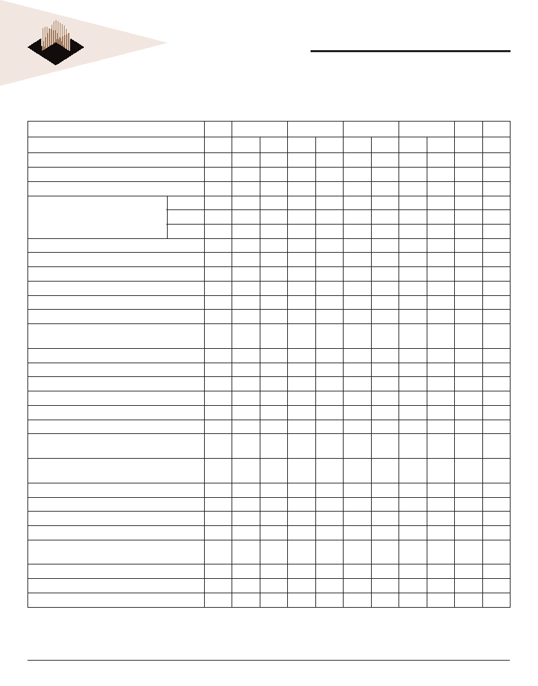
DDR SDRAM COMPONENT ELECTRICAL CHARACTERISTICS AND
RECOMMENDED AC OPERATING CONDITIONS
DDR400: VCC = VCCQ = +2.6V ± 0.1V; DDR333, 266: VCC = VCCQ = +2.5V ± 0.2V
AC Characteristics
403
335
262
265
Parameter
Symbol
Min
Max
Min
Max
Min
Max
Min
Max
Units
Notes
Access window of DQs from CK, CK#
tAC
-0.70
+0.70
-0.70
+0.70
-0.75
+0.75
-0.75
+0.75
ns
CK high-level width
tCH
0.45
0.55
0.45
0.55
0.45
0.55
0.45
0.55
tCK
16
CK low-level width
tCL
0.45
0.55
0.45
0.55
0.45
0.55
0.45
0.55
tCK
16
Clock cycle time
CL=3
tCK (3)
5
7.5
6
13
7.5
13
7.5
13
ns
22
CL=2.5 tCK (2.5)
6
12
6
12
7.5
12
7.5
12
ns
22
CL=2
tCK (2)
7.5
12
7.5
12
7.5
12
10
12
ns
22
DQ and DM input hold time relative to DQS
tDH
0.40
0.45
0.5
ns
14,17
DQ and DM input setup time relative to DQS
tDS
0.40
0.45
0.5
ns
14,17
DQ and DM input pulse width (for each input)
tDIPW
1.75
ns
17
Access window of DQS from CK, CK#
tDQSCK
-0.60
+0.60
-0.60
+0.60
-0.75
+0.75
-0.75
+0.75
ns
DQS input high pulse width
tDQSH
0.35
tCK
DQS input low pulse width
tDQSL
0.35
tCK
DQS-DQ skew, DQS to last DQ valid, per group,
per access
tDQSQ
0.40
0.45
0.5
ns
13,14
Write command to rst DQS latching transition
tDQSS
0.72
1.28
0.75
1.25
0.75
1.25
0.75
1.25
tCK
DQS falling edge to CK rising - setup time
tDSS
0.2
tCK
DQS falling edge from CK rising - hold time
tDSH
0.2
tCK
Half clock period
tHP
tCH, tCL
ns
18
Data-out high-impedance window from CK, CK#
tHZ
+0.70
+0.75
ns
8,19
Data-out low-impedance window from CK, CK#
tLZ
-0.70
-0.75
ns
8,20
Address and control input hold time
(slew rate >/ =.5V/ns)
tIHf
0.60
0.75
0.90
ns
6
Address and control input set-up time
(slew rate >/ =.5V/ns)
tISf
0.60
0.75
0.90
ns
6
Address and control input hold time (slow slew rate)
tIHs
N/A
0.80
1
ns
6
Address and control input setup time (slow slew rate)
tISs
N/A
0.80
1
ns
6
Address and control input pulse width (for each input)
tIPW
2.2
ns
LOAD MODE REGISTER command cycle time
tMRD
10
12
15
ns
DQ-DQS hold, DQS to rst DQ to go non-valid, per
access
tQH
tHP-tQHS
ns
13,14
Data hold skew factor
tQHS
0.55
0.75
ns
ACTIVE to PRECHARGE command
tRAS
40
70,000
42
70,000
40
120,000
40
120,000
ns
15
ACTIVE to READ with Auto precharge command
tRAP
15
ns
Note:
These parameters serve to support both
SAMSUNG and MICRON components based modules.
Continued on next page
相關(guān)PDF資料 |
PDF描述 |
|---|---|
| W3EG6433S265JD3 | 32M X 64 DDR DRAM MODULE, 0.75 ns, DMA184 |
| WS512K32-100HSI | 2M X 8 MULTI DEVICE SRAM MODULE, 100 ns, CHIP66 |
| WS512K32-35HC | 2M X 8 MULTI DEVICE SRAM MODULE, 35 ns, CHIP66 |
| WF128K32-120G4M5 | 512K X 8 FLASH 5V PROM MODULE, 120 ns, CQFP68 |
| WF128K32-120G4I5 | 512K X 8 FLASH 5V PROM MODULE, 120 ns, CQFP68 |
相關(guān)代理商/技術(shù)參數(shù) |
參數(shù)描述 |
|---|---|
| W3EG2128M72AFSR265D3XG | 制造商:WEDC 制造商全稱:White Electronic Designs Corporation 功能描述:2GB - 2x128Mx72 DDR SDRAM REGISTERED ECC, w/PLL, FBGA |
| W3EG2128M72AFSR335AD3XG | 制造商:WEDC 制造商全稱:White Electronic Designs Corporation 功能描述:2GB - 2x128Mx72 DDR SDRAM REGISTERED ECC, w/PLL, FBGA |
| W3EG2128M72AFSR403AD3XG | 制造商:WEDC 制造商全稱:White Electronic Designs Corporation 功能描述:2GB - 2x128Mx72 DDR SDRAM REGISTERED ECC, w/PLL, FBGA |
| W3EG2128M72AFSR-AD3 | 制造商:WEDC 制造商全稱:White Electronic Designs Corporation 功能描述:2GB - 2x128Mx72 DDR SDRAM REGISTERED ECC, w/PLL, FBGA |
| W3EG2128M72AFSR-D3 | 制造商:WEDC 制造商全稱:White Electronic Designs Corporation 功能描述:2GB - 2x128Mx72 DDR SDRAM REGISTERED ECC, w/PLL, FBGA |
發(fā)布緊急采購(gòu),3分鐘左右您將得到回復(fù)。