- 您現(xiàn)在的位置:買賣IC網(wǎng) > PDF目錄202134 > W25Q32BVZEAG (WINBOND ELECTRONICS CORP) 32M X 1 SPI BUS SERIAL EEPROM, PDSO8 PDF資料下載
參數(shù)資料
| 型號(hào): | W25Q32BVZEAG |
| 廠商: | WINBOND ELECTRONICS CORP |
| 元件分類: | PROM |
| 英文描述: | 32M X 1 SPI BUS SERIAL EEPROM, PDSO8 |
| 封裝: | 8 X 6 MM, GREEN, WSON-8 |
| 文件頁(yè)數(shù): | 53/79頁(yè) |
| 文件大?。?/td> | 1090K |
| 代理商: | W25Q32BVZEAG |
第1頁(yè)第2頁(yè)第3頁(yè)第4頁(yè)第5頁(yè)第6頁(yè)第7頁(yè)第8頁(yè)第9頁(yè)第10頁(yè)第11頁(yè)第12頁(yè)第13頁(yè)第14頁(yè)第15頁(yè)第16頁(yè)第17頁(yè)第18頁(yè)第19頁(yè)第20頁(yè)第21頁(yè)第22頁(yè)第23頁(yè)第24頁(yè)第25頁(yè)第26頁(yè)第27頁(yè)第28頁(yè)第29頁(yè)第30頁(yè)第31頁(yè)第32頁(yè)第33頁(yè)第34頁(yè)第35頁(yè)第36頁(yè)第37頁(yè)第38頁(yè)第39頁(yè)第40頁(yè)第41頁(yè)第42頁(yè)第43頁(yè)第44頁(yè)第45頁(yè)第46頁(yè)第47頁(yè)第48頁(yè)第49頁(yè)第50頁(yè)第51頁(yè)第52頁(yè)當(dāng)前第53頁(yè)第54頁(yè)第55頁(yè)第56頁(yè)第57頁(yè)第58頁(yè)第59頁(yè)第60頁(yè)第61頁(yè)第62頁(yè)第63頁(yè)第64頁(yè)第65頁(yè)第66頁(yè)第67頁(yè)第68頁(yè)第69頁(yè)第70頁(yè)第71頁(yè)第72頁(yè)第73頁(yè)第74頁(yè)第75頁(yè)第76頁(yè)第77頁(yè)第78頁(yè)第79頁(yè)
W25Q32BV
Publication Release Date: April 01, 2011
- 57 -
Revision F
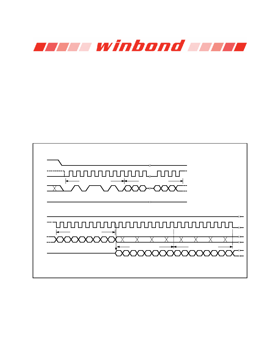
7.2.36 Read SFDP Register (5Ah)
The W25Q32BV features a 256-Byte Serial Flash Discoverable Parameter (SFDP) register that contains
information about device configurations, available instructions and other features. The SFDP parameters
are stored in one or more Parameter Identification (PID) tables. Currently only one PID table is specified,
but more may be added in the future. The Read SFDP Register instruction is compatible with the SFDP
standard initially established in 2010 for PC and other applications, as well as the JEDEC standard 1.0
that is published in 2011. Most Winbond SpiFlash Memories shipped after June 2011 (date code 1124
and beyond) support the SFDP feature as specified in the applicable datasheet.
The Read SFDP instruction is initiated by driving the /CS pin low and shifting the instruction code “5Ah”
followed by a 24-bit address (A23-A0)
(1) into the DI pin. Eight “dummy” clocks are also required before the
SFDP register contents are shifted out on the falling edge of the 40
th CLK with most significant bit (MSB)
first as shown in Figure 34. For SFDP register values and descriptions, refer to the following SFDP
Definition table.
Note: 1. A23-A8 = 0; A7-A0 are used to define the starting byte address for the 256-Byte SFDP Register.
/CS
CLK
DI
(IO
0)
DO
(IO
1)
Mode 0
Mode 3
0
1
2
3
4
5
6
7
Instruction (5Ah)
High Impedance
8
9
10
28
29
30
31
24-Bit Address
23
22
21
3
2
1
0
Data Out 1
*
/CS
CLK
DI
(IO
0)
32
DO
(IO
1)
33
34
35
36
37
38
39
Dummy Byte
High Impedance
40
41
42
44
45
46
47
48
49
50
51
52
53
54
55
7
6
5
4
3
2
1
0
7
Data Out 2
7
6
5
4
3
2
1
0
43
31
0
*
7
6
5
4
3
2
1
0
*
= MSB
*
Figure 34. Read SFDP Register Instruction Sequence Diagram
相關(guān)PDF資料 |
PDF描述 |
|---|---|
| W3EG6466S335AD4M | 64M X 64 DDR DRAM MODULE, 0.7 ns, DMA200 |
| W3EG7264S335AD4SG | 64M X 72 DDR DRAM MODULE, 0.7 ns, DMA200 |
| WF1M32B-120G2UI3A | 1M X 32 FLASH 3.3V PROM MODULE, 120 ns, CQFP68 |
| WF1M32B-120H1I3A | 1M X 32 FLASH 3.3V PROM MODULE, 120 ns, CPGA66 |
| WE128K32N-150G2TC | 128K X 32 EEPROM 5V MODULE, 125 ns, CQFP68 |
相關(guān)代理商/技術(shù)參數(shù) |
參數(shù)描述 |
|---|---|
| W25Q32BVZEAP | 制造商:WINBOND 制造商全稱:Winbond 功能描述:3V 32M-BIT SERIAL FLASH MEMORY WITH DUAL AND QUAD SPI |
| W25Q32BVZEIG | 制造商:Winbond Electronics Corp 功能描述:32MB SPI FLASH |
| W25Q32BVZEIP | 制造商:WINBOND 制造商全稱:Winbond 功能描述:3V 32M-BIT SERIAL FLASH MEMORY WITH DUAL AND QUAD SPI |
| W25Q32BVZPAG | 制造商:WINBOND 制造商全稱:Winbond 功能描述:3V 32M-BIT SERIAL FLASH MEMORY WITH DUAL AND QUAD SPI |
| W25Q32BVZPAP | 制造商:WINBOND 制造商全稱:Winbond 功能描述:3V 32M-BIT SERIAL FLASH MEMORY WITH DUAL AND QUAD SPI |
發(fā)布緊急采購(gòu),3分鐘左右您將得到回復(fù)。