- 您現(xiàn)在的位置:買賣IC網(wǎng) > PDF目錄203624 > W19B160BTB7H (WINBOND ELECTRONICS CORP) 1M X 16 FLASH 2.7V PROM, 7 ns, PBGA48 PDF資料下載
參數(shù)資料
| 型號(hào): | W19B160BTB7H |
| 廠商: | WINBOND ELECTRONICS CORP |
| 元件分類: | PROM |
| 英文描述: | 1M X 16 FLASH 2.7V PROM, 7 ns, PBGA48 |
| 封裝: | 6 X 8 MM, 0.80 MM PITCH, GREEN, TFBGA-48 |
| 文件頁(yè)數(shù): | 17/47頁(yè) |
| 文件大小: | 628K |
| 代理商: | W19B160BTB7H |
第1頁(yè)第2頁(yè)第3頁(yè)第4頁(yè)第5頁(yè)第6頁(yè)第7頁(yè)第8頁(yè)第9頁(yè)第10頁(yè)第11頁(yè)第12頁(yè)第13頁(yè)第14頁(yè)第15頁(yè)第16頁(yè)當(dāng)前第17頁(yè)第18頁(yè)第19頁(yè)第20頁(yè)第21頁(yè)第22頁(yè)第23頁(yè)第24頁(yè)第25頁(yè)第26頁(yè)第27頁(yè)第28頁(yè)第29頁(yè)第30頁(yè)第31頁(yè)第32頁(yè)第33頁(yè)第34頁(yè)第35頁(yè)第36頁(yè)第37頁(yè)第38頁(yè)第39頁(yè)第40頁(yè)第41頁(yè)第42頁(yè)第43頁(yè)第44頁(yè)第45頁(yè)第46頁(yè)第47頁(yè)
W19B160BT/B DATA SHEET
- 24 -
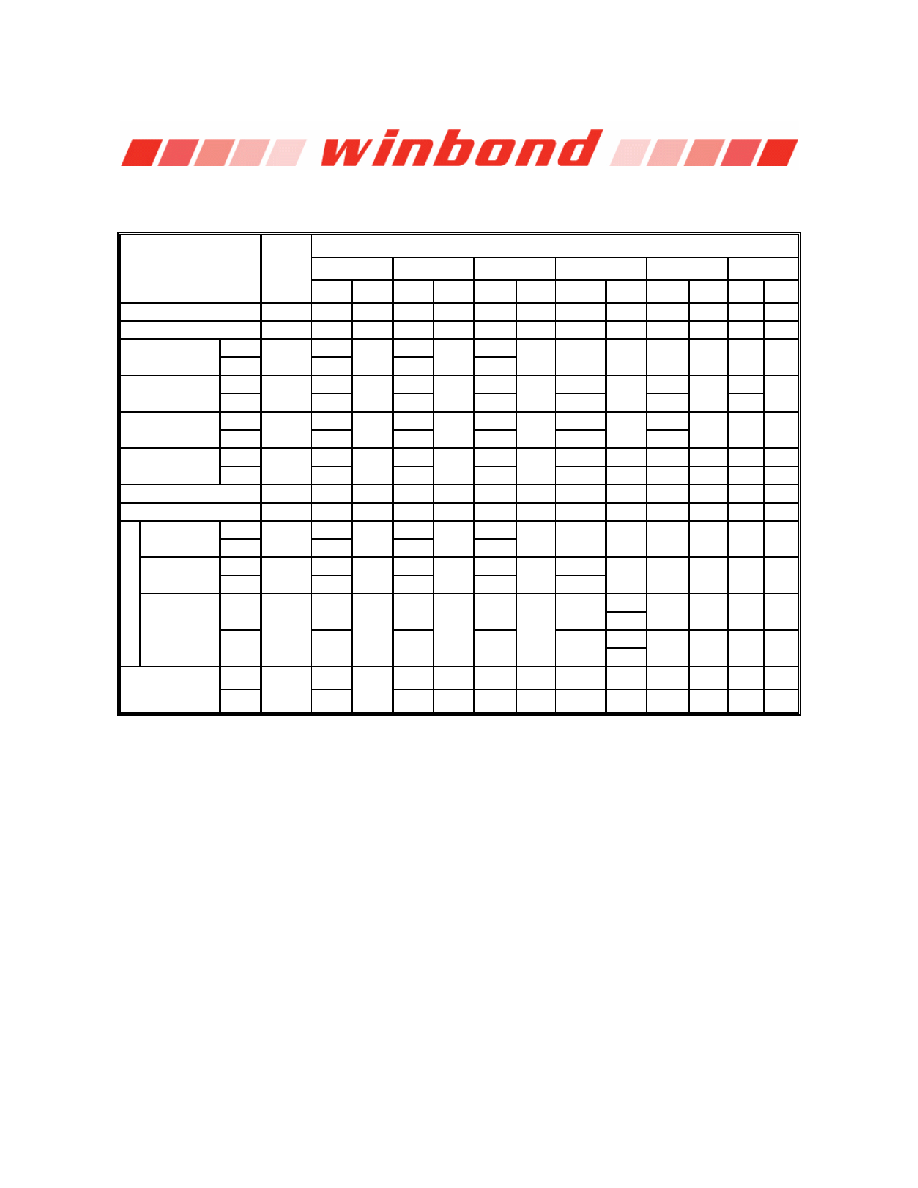
8.8 Command Definitions
BUS CYCLES (2-5)
FIRST
SECOND
THIRD
FOURTH
FIFTH
SIXTH
COMMAND
SEQUENCE
(1)
CYCLE
ADDR DATA ADDR DATA ADDR DATA ADDR DATA ADDR DATA ADDR DATA
Read (note 6)
1
RA
RD
Reset (note 7)
1
XXX
F0
Word
555
2AA
555
Normal
Program
Byte
4
AAA
AA
555
55
AAA
A0
PA
PD
Word
555
2AA
555
2AA
555
Chip Erase
Byte
6
AAA
AA
555
55
AAA
80
AAA
AA
555
55
AAA
10
Word
555
2AA
555
2AA
Sector Erase
Byte
6
AAA
AA
555
55
AAA
80
AAA
AA
555
55
SA
30
Word
555
2AA
555
Unlock pass
Byte
3
AAA
AA
555
55
AAA
20
Unlock bypass program
2
XXX
A0
PA
PD
Unlock bypass reset
2
XXX
90
XXX
F0
Word
555
2AA
555
Manufacturer
Code
Byte
4
AAA
AA
555
55
AAA
90
X00
DA
Word
555
2AA
555
X01
Device
Code
Byte
4
AAA
AA
555
55
AAA
90
x02
(note11
)
XX00
Word
555
2AA
555
(SA) X02
XX01
00
AUTO
SELECT(note8)
Sector Protect
Verify (note 9)
Byte
4
AAA
AA
555
55
AAA
90
(SA) X04
01
Word
55
Common Flash
Interface (CFI)
Query (note 10)
Byte
1
AA
98
Legend:
X = Don’t Care
RA = Address of the memory location to be read.
PA = Address of the memory location to be programmed. Addresses latch on the falling edge of the #WE or #CE pulse,
whichever happens later.
PD = Data to be programmed at location PA. Data latches on the rising edge of #WE or #CE pulse, whichever happens first.
RD = Data read from location RA during read operation.
SA = Address of the sector to be verified (in auto select mode) or erased. Address bits A19-A12 uniquely select any sector.
Notes:
1. See Bus Operations Table for details.
2. All values are in hexadecimal.
3. Except for the read cycle and the fourth cycle of the auto select command sequence, all bus cycles are write cycles.
4. Data bits DQ15-DQ8 are don’t care for unlock and command cycle.
5. Unless otherwise noted, address bits A19-A11 are don’t cares for unlock and command cycles.
6. No unlock or command cycles required when reading array data.
7. When device is in the auto select mode, the reset command is required to return to reading array data, or if DQ5 goes
high (while the device is providing status data).
8. The fourth cycle of the auto select command sequence is a read cycle.
9. The data is 00h for an unprotected sector and 01h for a protected sector.
相關(guān)PDF資料 |
PDF描述 |
|---|---|
| W23-X1A3Z-0.5 | PUSHBUTTON SWITCH, SPST, MOMENTARY, 0.5A, 50VDC, PANEL MOUNT |
| W31-X2M5Z-5 | TOGGLE SWITCH, SPST, LATCHED, 5A, 50VDC, PANEL MOUNT-THREADED |
| W31-X2M5Z-10 | TOGGLE SWITCH, SPST, LATCHED, 10A, 50VDC, PANEL MOUNT-THREADED |
| W31-X2M5Z-0.5 | TOGGLE SWITCH, SPST, LATCHED, 0.5A, 50VDC, PANEL MOUNT-THREADED |
| W31-X2M5G-50 | TOGGLE SWITCH, SPST, LATCHED, 50A, 50VDC, PANEL MOUNT-THREADED |
相關(guān)代理商/技術(shù)參數(shù) |
參數(shù)描述 |
|---|---|
| W19B160BTBH7H | 制造商:WINBOND 制造商全稱:Winbond 功能描述:16Mbit, 2.7~3.6 volt CMOS flash memory |
| W19B160BTBM7H | 制造商:WINBOND 制造商全稱:Winbond 功能描述:16Mbit, 2.7~3.6 volt CMOS flash memory |
| W19B160BTT7H | 制造商:WINBOND 制造商全稱:Winbond 功能描述:2.7~3.6-volt write (program and erase) operations, Fast write operation |
| W19B160TB7H7H | 制造商:WINBOND 制造商全稱:Winbond 功能描述:16Mbit, 2.7~3.6 volt CMOS flash memory |
| W19B160TB7M7H | 制造商:WINBOND 制造商全稱:Winbond 功能描述:16Mbit, 2.7~3.6 volt CMOS flash memory |
發(fā)布緊急采購(gòu),3分鐘左右您將得到回復(fù)。