- 您現(xiàn)在的位置:買(mǎi)賣(mài)IC網(wǎng) > PDF目錄221468 > VS-550-LFF-GNN-P2-R3 (VECTRON INTERNATIONAL) VOLTAGE CONTROLLED CLOCK SAW OSCILLATOR, 622.08 MHz PDF資料下載
參數(shù)資料
| 型號(hào): | VS-550-LFF-GNN-P2-R3 |
| 廠商: | VECTRON INTERNATIONAL |
| 元件分類(lèi): | XO, clock |
| 英文描述: | VOLTAGE CONTROLLED CLOCK SAW OSCILLATOR, 622.08 MHz |
| 封裝: | ROHS COMPLIANT, HERMETIC SEALED, J LEADED, 6 PIN |
| 文件頁(yè)數(shù): | 4/7頁(yè) |
| 文件大小: | 139K |
| 代理商: | VS-550-LFF-GNN-P2-R3 |
VS-550 Voltage Controlled SAW Oscillator
Vectron International, 267 Lowell Rd, Hudson NH 03051-4916
Tel: 1-88-VECTRON-1
Website: www.vectron.com
Page 4 of 7
Rev: 11Apr06
Absolute Maximum Ratings
Parameter
Symbol
Ratings
Unit
Power Supply
VCC
0 to 6
V
Input Current
IIN
100
mA
Output Current
IOUT
25
mA
Voltage Control Range
VC
0 to VCC
V
Storage Temperature
TSTR
-55 to 125
°C
Solder Temperature / Duration
TPEAK / tP
260 / 40
°C / sec
Stresses in excess of the absolute maximum ratings can permanently damage the device. Also, exposure to
these absolute maximum ratings for extended periods may adversely affect device reliability. Functional
operation is not implied at these or any other conditions in excess of those represented in the operational
sections of this datasheet. Permanent damage is also possible if any device input (Vc or FS) draws greater
than 100mA.
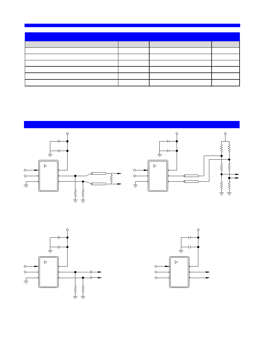
Suggested Output Load Configurations
LV-PECL to LV-PECL: For short transmission lengths, the power
consumption could be reduced by removing the 100
resistor and
doubling the value of the pull down resistors.
Functional Test: Allows standard power supply configuration.
Since AC coupled, the LV-PECL levels cannot be measured.
LV-PECL to LVDS: Restricted for short transmission lengths.
Configuration may require modification depending on LVDS receiver.
40
40
150
150
49
49
+3.3V
Production Test: Allows direct DC coupling into 50
measurement
equipment. Must bias the power supplies as shown. Similar to Figure 1.
0.01
F
0.01
F
16
2
34
5
Vc
FS
Gnd
+3.3V
0.01
F
0.10
F
Vcc
COutput
240
Output
240
100
Z = 50
Z = 50
Output
Gnd
34
Z = 50
+3.3V
0.10
F
FS
Vc
6
1
25
COutput
Vcc
0.01
F
Z = 50
Gnd
FS
Vc
4
3
Output
240
16
2
5
COutput
Vcc
0.01
F
+3.3V
0.10
F
240
-1.3V
FS
Vc
34
6
1
25
COutput
Output
Vcc
+2.0V
0.01
F
0.10
F
相關(guān)PDF資料 |
PDF描述 |
|---|---|
| VS-550-LFF-GNN-P2-R6 | VOLTAGE CONTROLLED CLOCK SAW OSCILLATOR, 622.08 MHz |
| VS-720-LPF-HAA-637.500 | VOLTAGE CONTROLLED CLOCK SAW OSCILLATOR, 637.5 MHz |
| VS-750-LFF-HNN-R1-R6 | VOLTAGE CONTROLLED CLOCK SAW OSCILLATOR, 669.6429 MHz |
| VS-750-LFF-HNN-R3-R1 | VOLTAGE CONTROLLED CLOCK SAW OSCILLATOR, 669.3266 MHz |
| VS-750-LFF-HNN-R3-T4 | VOLTAGE CONTROLLED CLOCK SAW OSCILLATOR, 669.3266 MHz |
相關(guān)代理商/技術(shù)參數(shù) |
參數(shù)描述 |
|---|---|
| VS-550-LFF-HNN | 制造商:未知廠家 制造商全稱(chēng):未知廠家 功能描述:DUAL FREQUENCY VCSO |
| VS-550-LFF-HNN-P2-P4 | 制造商:VECTRON 制造商全稱(chēng):Vectron International, Inc 功能描述:DUAL FREQUENCY VCSO |
| VS-562 | 制造商:Leach International Corporation 功能描述:VOLTAGE SENSOR - Bulk |
| VS-572 | 制造商:Leach International Corporation 功能描述:VOLTAGE SENSOR - Bulk |
| VS-576 | 制造商:Leach International Corporation 功能描述:757 , MD-11 AIR LINE - Bulk |
發(fā)布緊急采購(gòu),3分鐘左右您將得到回復(fù)。