- 您現(xiàn)在的位置:買賣IC網(wǎng) > PDF目錄361742 > VP16256-40 (Mitel Networks Corporation) Programmable FIR Filter PDF資料下載
參數(shù)資料
| 型號: | VP16256-40 |
| 廠商: | Mitel Networks Corporation |
| 英文描述: | Programmable FIR Filter |
| 中文描述: | 可編程FIR濾波器 |
| 文件頁數(shù): | 16/20頁 |
| 文件大?。?/td> | 228K |
| 代理商: | VP16256-40 |
16
VP16256
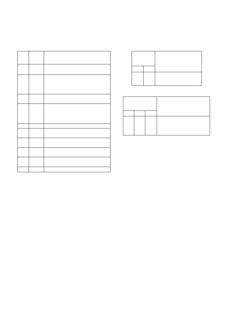
CONTROL REGISTER
The internal operation of the VP16256 is controlled by the
status of a 16-bit control register. In the dual filter modes both
networks are controlled by the same register. The significance
of the various bits are shown in Table 6. Tables 7 and 8 define
the control register bit interdependence for the filter and bank
swapping modes.
The control register is double buffered. This allows the
writing of a new control word without affecting the current
operation of the device. To activate the new control register
after it has been written to the device the bank swap signal must
be toggled. After a reset the active control register is loaded
directly and bank swap need not be used.
Control
Register
Bits
7
0
1
1
X
Function
6
X
0
1
X
5
0
0
0
1
Control by input pin
Lower bank selected
Upper bank selected
Swap on every sample clock
Table 8 Control register bank swap bits
Bits Decode
Function
15
15
0
1
00
01
10
11
0
1
00
01
10
11
00
0
1
0
1
0
1
0
1
Dual filter mode
Single filter mode
Sample rate is the system clock
Sample rate is half the system clock
Sample rate is quarter the system clock
Sample rate is eighth the system clock
Output rate equals the input rate
Decimate-by-two
Intermediate device
Interface device
Termination device
Single device
These bits MUST be at logical zero
Bank swap is controlled by input pin
Bank swap is controlled by Bit 6
Lower bank if bit 7 is set
Upper bank if bit 7 is set
Normal Bank Swap
Bank swap on every sample clock
Two independent filters
Two filters in cascade
These bits MUST be at logical zero
14:13
14:13
14:13
14:13
12
12
11:10
11:10
11:10
11:10
9:8
7
7
6
6
5
5
4
4
3:0
Control
Register
Bits
15
0
0
1
Function
4
0
1
X
Two independent filters
Two filters in cascade
Single Filter
Table 7 Control register filter mode bits
ABSOLUTE MAXIMUM RATINGS (Note 1)
Supply voltage V
DD
Input voltage V
Output voltage V
Clamp diode current per pin I
K
(see note 2)
Static discharge voltage (HBM)
Storage temperature T
Ambient temperature with power applied T
AMB
0
°
C to
1
70
°
C
Junction temperature with power applied T
J
Package power dissipation
Thermal resistance, junction-to-case
θ
JC
2
0·5V to
1
7·0V
2
0·5V to V
DD
1
0·5V
2
0·5V to V
DD
1
0·5V
18mA
500V
2
65
°
C to
1
150
°
C
120
°
C
2500mW
1·0
°
C/W
NOTES
1. Exceeding these ratings may cause permanent damage.
Functional operation under these conditions is not implied.
2. Maximum dissipation should not be exceeded for more
than1 second, only one output to be tested at any one time.
3. Exposure to absolute maximum ratings for extended
periods may affect device reliablity.
4. Current is defined as negative into the device.
5. The
θ
data assumes that heat is extracted from the
bottom of the package via the integral heat sink.
6. The metal ‘heat slug’ in the base of the package is
connected to the substrate, which is at V
DD
potential.
Table 6 Control register bit allocation
相關(guān)PDF資料 |
PDF描述 |
|---|---|
| VP16256-40CGGH1N | Programmable FIR Filter |
| VP16256 | Programmable FIR Filter |
| VP16256-27 | Programmable FIR Filter |
| VP16256-27CG | Programmable FIR Filter |
| VP16256-40CG | Programmable FIR Filter |
相關(guān)代理商/技術(shù)參數(shù) |
參數(shù)描述 |
|---|---|
| VP16256-40/CG/GH1N | 制造商:ZARLINK 制造商全稱:Zarlink Semiconductor Inc 功能描述:Programmable FIR FIlter |
| VP16256-40CG | 制造商:MITEL 制造商全稱:Mitel Networks Corporation 功能描述:Programmable FIR Filter |
| VP16256-40CGGH1N | 制造商:MITEL 制造商全稱:Mitel Networks Corporation 功能描述:Programmable FIR Filter |
| VP16256-40CGGH1R | 制造商:未知廠家 制造商全稱:未知廠家 功能描述:Digital Filter |
| VP165/24 | 制造商:Smarteq Wireless Ab 功能描述: |
發(fā)布緊急采購,3分鐘左右您將得到回復(fù)。