- 您現(xiàn)在的位置:買(mǎi)賣(mài)IC網(wǎng) > PDF目錄359397 > VN02AN (意法半導(dǎo)體) INDUCTOR KIT, B82462 SERIES; RoHS Compliant: Yes PDF資料下載
參數(shù)資料
| 型號(hào): | VN02AN |
| 廠商: | 意法半導(dǎo)體 |
| 英文描述: | INDUCTOR KIT, B82462 SERIES; RoHS Compliant: Yes |
| 中文描述: | 高邊智能電源固態(tài)繼電器 |
| 文件頁(yè)數(shù): | 5/11頁(yè) |
| 文件大?。?/td> | 104K |
| 代理商: | VN02AN |
FUNCTIONAL DESCRIPTION
The device has a
indicatesover temperatureconditions.
The truth table shows input, diagnostic output
status and
output voltage
operation and fault conditions. The output signals
are processedby internal logic.
To protect the device against short circuit and
over current conditions, the thermal protection
turns the integratedPower MOS off ata minimum
junction temperature of 140
temperature returns to 125
automatically turned on again. To ensure the
protection in all V
CC
conditions and in all the
junction temperaturerange it is necessary to limit
the voltage drop across Drain and Source (pin 3
and 5) at 28V accordingto:
V
ds
= V
CC
- I
OV
* (R
i
+ R
w
+ R
l
)
where:
R
i
= internalresistence of Power Supply
R
w
= Wires resistance
R
l
= Short Circuit resistance
Driving inductiveloads, an internal function of the
device ensures the fast demagnetization with
typical voltage (V
demag
) of -18V.
This function allows the reduction of the power
dissipation according to the formula:
P
dem
= 0.5 * L
load
* (I
load
)
2
* [(V
CC
+ V
dem
)/V
dem
] * f
diagnostic output which
level
in
normal
o
C. When the
o
C the switch is
where f = Switching Frequency
Based on this formula it is possible to know the
value of inductance and/or current to avoid a
thermalshut-down.
PROTECTING THE DEVICE AGAINST RE-
VERSEBATTERY
The simpliest way to protect the device against a
continuous reverse battery voltage (-36V) is to
insert a Schottky diode between pin 1 (GND)and
ground, as shown in the typical application circuit
(Fig. 3). The consequences of the voltage drop
across this diode areas follows:
If the input is pulled to power GND, a negative
voltage of -V
f
is seen by the device. (V
il
, V
ih
thresholds and Vstat are increased by V
f
with
respectto power GND).
The undervoltageshut-down level is increased by
V
f
.
If there is no need for the control unit to handle
external analog signals referred to the power
GND, the best approach is to connect the
reference potential of the control unit to node [1]
(see application circuit in fig. 4), which becomes
the common signal GND for the whole control
board avoiding shift of V
ih
, V
il
and V
stat
. This
solutionallows the use of a standard diode.
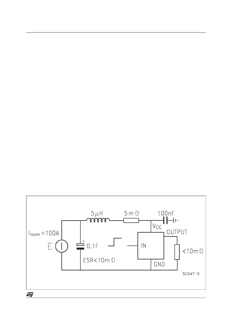
Figure2:
Over CurrentTest Circuit
VN02AN
5/11
相關(guān)PDF資料 |
PDF描述 |
|---|---|
| VN02ANSP | HIGH SIDE SMART POWER SOLID STATE RELAY |
| VN02HSP13TR | HIGH SIDE SMART POWER SOLID STATE RELAY |
| VN02HSP | High Side Smart Power Solid State Relay(高邊智能化功率固態(tài)繼電器) |
| VN02H | High Side Smart Power Solid State Relay(高邊智能化功率固態(tài)繼電器) |
| VN02NPT | HIGH SIDE SMART POWER SOLID STATE RELAY |
相關(guān)代理商/技術(shù)參數(shù) |
參數(shù)描述 |
|---|---|
| VN02AN(011Y) | 制造商:STMicroelectronics 功能描述: |
| VN02AN(012Y) | 制造商:STMICROELECTRONICS 制造商全稱(chēng):STMicroelectronics 功能描述:HIGH SIDE SMART POWER SOLID STATE RELAY |
| VN02AN011Y | 制造商:STMICROELECTRONICS 制造商全稱(chēng):STMicroelectronics 功能描述:HIGH SIDE SMART POWER SOLID STATE RELAY |
| VN02AN012Y | 制造商:STMICROELECTRONICS 制造商全稱(chēng):STMicroelectronics 功能描述:HIGH SIDE SMART POWER SOLID STATE RELAY |
| VN02AN-11-E | 功能描述:電源開(kāi)關(guān) IC - 配電 High Side Relay Pentawatt 5 Auto RoHS:否 制造商:Exar 輸出端數(shù)量:1 開(kāi)啟電阻(最大值):85 mOhms 開(kāi)啟時(shí)間(最大值):400 us 關(guān)閉時(shí)間(最大值):20 us 工作電源電壓:3.2 V to 6.5 V 電源電流(最大值): 最大工作溫度:+ 85 C 安裝風(fēng)格:SMD/SMT 封裝 / 箱體:SOT-23-5 |
發(fā)布緊急采購(gòu),3分鐘左右您將得到回復(fù)。