- 您現(xiàn)在的位置:買賣IC網(wǎng) > PDF目錄359372 > VFC101JN Synchronized VOLTAGE-TO-FREQUENCY CONVERTER PDF資料下載
參數(shù)資料
| 型號(hào): | VFC101JN |
| 英文描述: | Synchronized VOLTAGE-TO-FREQUENCY CONVERTER |
| 中文描述: | 同步電壓頻率轉(zhuǎn)換器 |
| 文件頁(yè)數(shù): | 3/10頁(yè) |
| 文件大?。?/td> | 136K |
| 代理商: | VFC101JN |
3
VFC101
SPECIFICATIONS
(CONT)
ELECTRICAL
At T
A
= +25
°
C and
±
15VDC supplies unless otherwise noted.
VFC101JN
VFC101KN
PARAMETER
CONDITIONS
MIN
TYP
MAX
MIN
TYP
MAX
UNITS
TEMPERATURE RANGE
Specification
Storage
θ
JA
θ
JC
0
+70
+150
*
*
*
*
°
C
°
C
–65
90
35
*
*
°
C/W
°
C/W
* Specification same as JN grade.
NOTES: (1) Offset and gain error can be trimmed to zero. (2) Specified by the box method: (max – min)
÷
(Avg x
T).
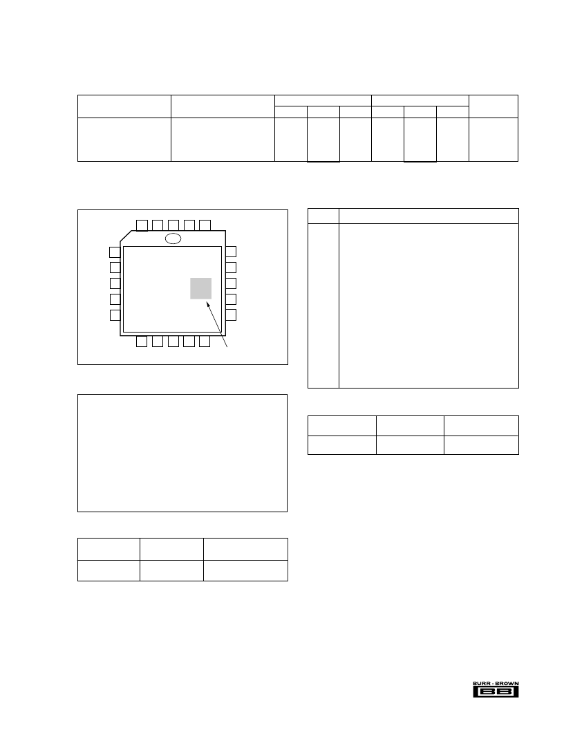
PIN CONFIGURATION
Top View
PIN #
DESCRIPTION
1
2
3
4
5
6
7
8
9
10
11
12
13
14
15
16
17
18
19
20
NC
+V
CC
Power Supply
NC
V
OUT
Integrator Amp Output
C
INT
, Integrator Inverting Input
+V
, Integrator Noninverting Input
V
IN
, 5V FS
V
IN
, 10V FS
V
IN
, 8V FS
V
IN
, 10V FS
–V
CC
Power Supply
C
OS
, Output One-Shot Capacitor
f
CLOCK
Input
f
Frequency Output
Digital Ground
Analog Ground
– Comparator Input
+ Comparator Input
NC
V
REF
+5V Reference Output
PIN ASSIGNMENTS
ABSOLUTE MAXIMUM RATINGS
Power Supply Voltage (+V
to –V
) .................................................36V
+V
CC
to Analog Common .....................................................................28V
–V
CC
to Analog Common......................................................................28V
Integrator Out Short-Circuit to Ground ........................................Indefinite
Integrator Differential Input ................................................................
±
10V
Integrator Common-Mode Input .................................... –V
CC
+5V to +2V
V
IN
(pins 7, 8, 9, 10) ..........................................................................
±
V
CC
Clock Input .........................................................................................
±
V
CC
V
REF
Out Short-Circuit to Ground .................................................Indefinite
C
OS
(Pin 12) ................................................................................0 to +V
CC
f
OUT
(referred to digital common)........................................... –0.5V to 36V
Digital Common .................................................................................
±
V
CC
Storage Temperature Range ..........................................–65
°
C to +150
°
C
Lead Temperature (soldering, 10s) ............................................... +300
°
C
PACKAGE INFORMATION
(1)
PACKAGE DRAWING
NUMBER
MODEL
PACKAGE
VFC101JN
VFC101KN
20-Pin PLCC
20-Pin PLCC
181
181
NOTE: (1) For detailed drawing and dimension table, please see end of data
sheet, or Appendix D of Burr-Brown IC Data Book.
ORDERING INFORMATION
MODEL
PACKAGE
TEMPERATURE RANGE
VFC101JN
VFC101KN
20-Pin PLCC
20-Pin PLCC
0
°
C to +70
°
C
0
°
C to +70
°
C
The information provided herein is believed to be reliable; however, BURR-BROWN assumes no responsibility for inaccuracies or omissions. BURR-BROWN assumes
no responsibility for the use of this information, and all use of such information shall be entirely at the user’s own risk. Prices and specifications are subject to change
without notice. No patent rights or licenses to any of the circuits described herein are implied or granted to any third party. BURR-BROWN does not authorize or warrant
any BURR-BROWN product for use in life support devices and/or systems.
20-Pin
PLCC
Package
Grade
Designation
3
2
1
20
19
9
10
11
12
13
4
5
6
7
8
18
17
16
15
14
相關(guān)PDF資料 |
PDF描述 |
|---|---|
| VFC101KN | Synchronized VOLTAGE-TO-FREQUENCY CONVERTER |
| VFC110 | High-Frequency VOLTAGE-TO-FREQUENCY CONVERTER |
| VFC110AG | High-Frequency VOLTAGE-TO-FREQUENCY CONVERTER |
| VFC110AP | High-Frequency VOLTAGE-TO-FREQUENCY CONVERTER |
| VFC110BG | High-Frequency VOLTAGE-TO-FREQUENCY CONVERTER |
相關(guān)代理商/技術(shù)參數(shù) |
參數(shù)描述 |
|---|---|
| VFC101KN | 制造商:BB 制造商全稱:BB 功能描述:Synchronized VOLTAGE-TO-FREQUENCY CONVERTER |
| VFC110 | 制造商:BB 制造商全稱:BB 功能描述:High-Frequency VOLTAGE-TO-FREQUENCY CONVERTER |
| VFC-1106 | 制造商:Quest Technology International Inc 功能描述: |
| VFC110AG | 功能描述:電壓頻率轉(zhuǎn)換及頻率電壓轉(zhuǎn)換 Hi f V to f RoHS:否 制造商:Texas Instruments 全標(biāo)度頻率:4000 KHz 線性誤差:+/- 1 % FSR 電源電壓-最大: 電源電壓-最小: 最大工作溫度:+ 85 C 最小工作溫度:- 25 C 安裝風(fēng)格:Through Hole 封裝 / 箱體:PDIP-14 封裝:Tube |
| VFC110AP | 功能描述:電壓頻率轉(zhuǎn)換及頻率電壓轉(zhuǎn)換 VOLTAGE-TO-FREQUENCY CONVERTER RoHS:否 制造商:Texas Instruments 全標(biāo)度頻率:4000 KHz 線性誤差:+/- 1 % FSR 電源電壓-最大: 電源電壓-最小: 最大工作溫度:+ 85 C 最小工作溫度:- 25 C 安裝風(fēng)格:Through Hole 封裝 / 箱體:PDIP-14 封裝:Tube |
發(fā)布緊急采購(gòu),3分鐘左右您將得到回復(fù)。