- 您現(xiàn)在的位置:買賣IC網(wǎng) > PDF目錄359372 > VFC101 Synchronized VOLTAGE-TO-FREQUENCY CONVERTER PDF資料下載
參數(shù)資料
| 型號: | VFC101 |
| 英文描述: | Synchronized VOLTAGE-TO-FREQUENCY CONVERTER |
| 中文描述: | 同步電壓頻率轉(zhuǎn)換器 |
| 文件頁數(shù): | 5/10頁 |
| 文件大小: | 136K |
| 代理商: | VFC101 |
5
VFC101
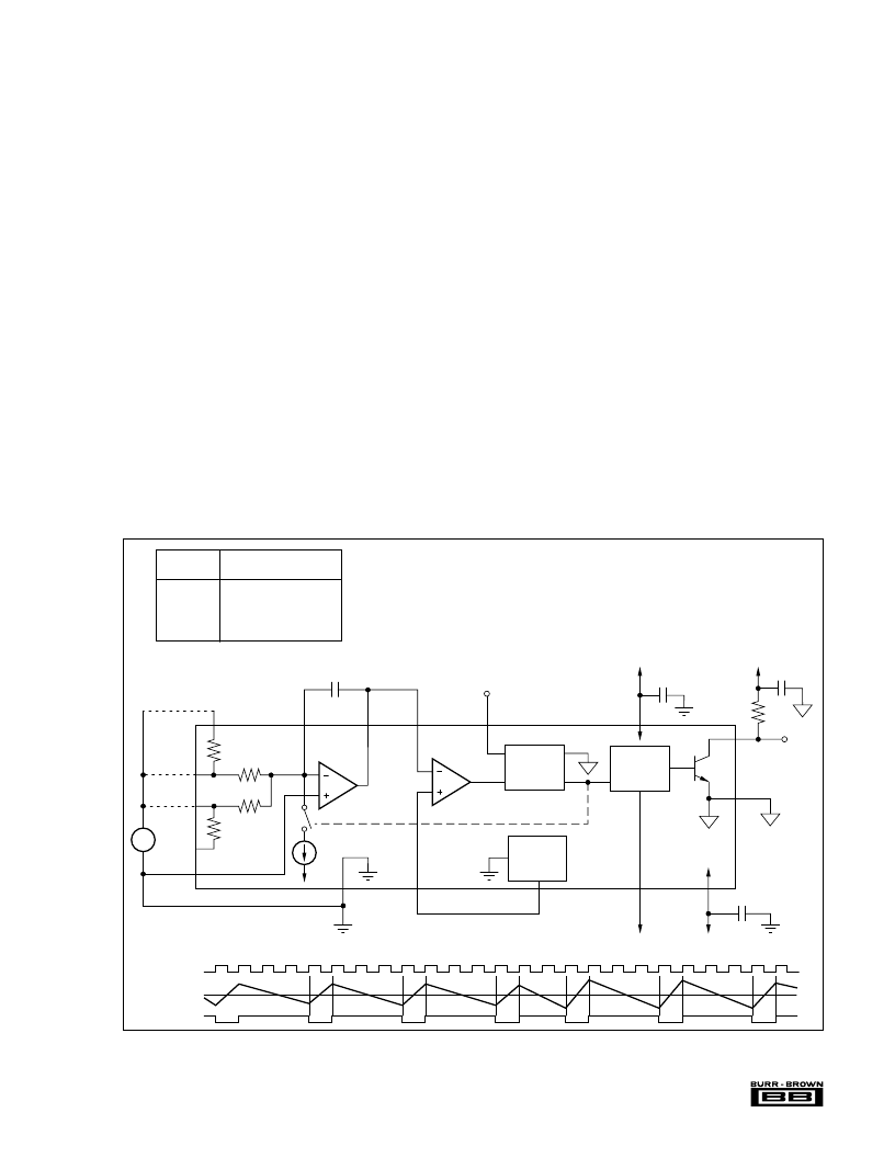
THEORY OF OPERATION
The VFC101 voltage-to-frequency converter provides digi-
tal output pulses with an average frequency proportional to
the analog input voltage. The output is an active low pulse
of constant duration, with a repetition rate determined by the
input voltage. Falling edges of the output pulses are synchro-
nized with rising edges of the clock input.
Operation is similar to a conventional charge-balance VFC.
An input operational amplifier (Figure 1) is configured as an
integrator so that a positive input voltage causes an input
current to flow in C
. This forces the integrator output to
ramp negatively. When the output of the integrator crosses
the reference voltage (5V), the comparator trips, activating
the clocked logic circuit. Once activated, the clocked logic
awaits a falling edge of the clock input, followed by a rising
edge. On the rising edge, switch SW
is closed for one
complete clock cycle, causing the reset current, I
, to switch
to the integrator input. Since I
is larger than the input
current, I
, the output of the integrator ramps positively
during the one clock cycle reset period. The clocked logic
circuitry also generates a VFC output pulse during the reset
period.
Unlike conventional VFC circuits, the VFC101 accurately
derives its reset period from an external clock frequency.
This eliminates the critical timing capacitor required by
other VFC circuits. One period (from rising edge to rising
edge) of the clock input determines the integrator reset
period.
When the negative-going integration of the input signal
crosses the comparator threshold, integration of the input
signal will continue until the reset period can start (awaiting
the necessary transitions of the clock). Output pulses are
thus made to align with rising edges of the external clock.
This causes the instantaneous output frequency to be a
subharmonic of the clock frequency. The average frequency,
however, will be an accurate analog of the input voltage.
A full-scale input causes a nominal output frequency equal
to one-half the clock frequency. The transfer function is
f
OUT
= (V
IN
/2V
FS
) f
CLOCK
.
Input voltages greater than V
FS
cause the output frequency
to limit at half the clock frequency. Negative inputs cause all
output pulses to cease. The full-scale input voltage, V
FS
, is
determined by the input pin used—see Figure 1.
One of the useful functions made possible by the VFC101’s
multiple input resistors is shown in Figure 2. By connecting
one 10V input to the 5V V
REF
output, the other 10V input pin
functions as a bipolar input. A –5V to +5V input range
causes a zero to f
/2 output frequency range. Accurate
ratio matching and temperature tracking of the input resis-
tors provides improved stability of the half-scale offset.
FIGURE 1. Basic Voltage-to-Frequency Operations.
Integrator
Comparator
Clocked
Logic
Output
One-Shot
5
4
17
13
SW
1
1mA
18
2
+V
CC
14
15
f
OUT
0 to f
CLOCK/2
Digital
Ground
12
11
–V
CC
16
Analog
Ground
5V
Reference
20
C
INT
0.1μF
+V
L
0.1μF
+V
CC
f
CLOCK
TTL/CMOS
I
1
+V
CC
0.1μF
–V
CC
–V
CC
Integrator 5V
Clock
O
f
7
9
10k
8
10k
16k
10
4k
6
V
IN
0 to 10V
0 to 5V
0 to 8V
INPUT
Pin Number
8
10
9
7
7
(1)
NOTE: (1) Pin 8 connected to pin 5.
FULL-SCALE VOLTAGE
V
RS
10V
10V
8V
5V
2.5V
相關(guān)PDF資料 |
PDF描述 |
|---|---|
| VFC101JN | Synchronized VOLTAGE-TO-FREQUENCY CONVERTER |
| VFC101KN | Synchronized VOLTAGE-TO-FREQUENCY CONVERTER |
| VFC110 | High-Frequency VOLTAGE-TO-FREQUENCY CONVERTER |
| VFC110AG | High-Frequency VOLTAGE-TO-FREQUENCY CONVERTER |
| VFC110AP | High-Frequency VOLTAGE-TO-FREQUENCY CONVERTER |
相關(guān)代理商/技術(shù)參數(shù) |
參數(shù)描述 |
|---|---|
| VFC101JN | 制造商:BB 制造商全稱:BB 功能描述:Synchronized VOLTAGE-TO-FREQUENCY CONVERTER |
| VFC101KN | 制造商:BB 制造商全稱:BB 功能描述:Synchronized VOLTAGE-TO-FREQUENCY CONVERTER |
| VFC110 | 制造商:BB 制造商全稱:BB 功能描述:High-Frequency VOLTAGE-TO-FREQUENCY CONVERTER |
| VFC-1106 | 制造商:Quest Technology International Inc 功能描述: |
| VFC110AG | 功能描述:電壓頻率轉(zhuǎn)換及頻率電壓轉(zhuǎn)換 Hi f V to f RoHS:否 制造商:Texas Instruments 全標度頻率:4000 KHz 線性誤差:+/- 1 % FSR 電源電壓-最大: 電源電壓-最小: 最大工作溫度:+ 85 C 最小工作溫度:- 25 C 安裝風(fēng)格:Through Hole 封裝 / 箱體:PDIP-14 封裝:Tube |
發(fā)布緊急采購,3分鐘左右您將得到回復(fù)。