- 您現(xiàn)在的位置:買賣IC網(wǎng) > PDF目錄361662 > V375A12T150B (Vicor Corporation) 375Vin / 12Vout / 150Watts DC-DC Converter Module PDF資料下載
參數(shù)資料
| 型號: | V375A12T150B |
| 廠商: | Vicor Corporation |
| 元件分類: | DC/DC變換器 |
| 英文描述: | 375Vin / 12Vout / 150Watts DC-DC Converter Module |
| 中文描述: | 375Vin / 12Vout / 150Watts DC - DC轉(zhuǎn)換模塊 |
| 文件頁數(shù): | 6/8頁 |
| 文件大小: | 142K |
| 代理商: | V375A12T150B |

Vicor Corp.
Tel: 800-735-6200, 978-470-2900 Fax: 978-475-6715
V375C12C150B DC-DC Converter
Rev. 3
Page 6 of 8
Set your site on VICOR at www.vicorpower.com
CONTROLFUNCTIONS - PR PIN
Parallel Operation
The PR pin supports paralleling for increased power with N+1
(N+M) redundancy and phased array capability. Modules of
the same input voltage, output voltage, and power level will
current share if all PR pins are suitably interfaced.
Compatible interface architectures include the following:
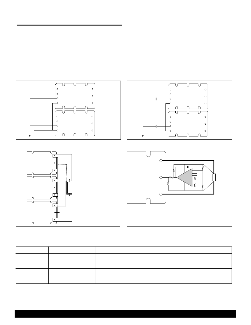
DC coupled single-wire interface.
All PR pins are directly
connected to one another. This interface supports current
sharing but is not fault tolerant. Minus In pins must be tied to
the same electric potential. See Figure 9.
AC coupled single-wire interface.
All PR pins are connected
to a single communication bus through 0.001μF (500V)
capacitors. This interface supports current sharing and is fault
tolerant except for the communication bus. See Figure 10.
Figure 9
—
DC coupled single-wire interface.
Module 2
(up to 12)
Module 1
Ground plane
+Out
SC
–
Out
+In
PC
PR
–
In
+Out
SC
–
Out
+In
PC
PR
–
In
Module 2
(up to 12)
Module 1
Ground plane
+Out
SC
–
Out
+In
PC
PR
–
In
+Out
SC
–
Out
+In
PC
PR
–
In
Figure 10
—
AC coupled single-wire interface.
0.001μF
0.001μF
R1
4
2
1
3
7
6
Load
LM10
+Out
SC
–
Out
R2
R3
8
1.05K
200
R4
1.2K
+Out
SC
–
Out
+Out
SC
–
Out
+Out
SC
–
Out
L
O
A
D
Plane
Ground
Plane
The +Out and
–
Out
power buses should be
designed to minimize
and balance parasitic
impedance from each
module output to the
load.
At the discretion of the
power system designer,
a subset of all modules
within an array may be
configured as slaves by
shorting SC to
–
Out.
Do not use output
OR
’
ing diodes with
MicroMods.
This module is designed for point of load regulation, where remote sensing
is not required.Active voltage drop compensator, as shown here, may be
used in applications with significant distribution losses.Details of this circuit
are available in the design guide.
Figure 12
—
Voltage drop compensation.
Figure 11
—
N+1 module array output connections.
PIN STYLES *
Designator
Description
Notes
(None)
Short solder
Requires in-board, mounting
L
Long solder
On-board mounting for 0.065" boards
S
Short ModuMate
SurfMate or in-board socket mounting
N
Long ModuMate
On-board socket mounting
* Pin style designator follows the
“
B
”
after the output power and precedes the baseplate designator.
Ex. V48B24C250BN
—
Long ModuMate Pins
相關(guān)PDF資料 |
PDF描述 |
|---|---|
| V375C12M150B | 375Vin / 12Vout / 150Watts DC-DC Converter Module |
| V375A12C150B | 375Vin / 12Vout / 150Watts DC-DC Converter Module |
| V375B12C150B | 375Vin / 12Vout / 150Watts DC-DC Converter Module |
| V375B12H150B | 375Vin / 12Vout / 150Watts DC-DC Converter Module |
| V375B12T150B | 375Vin / 12Vout / 150Watts DC-DC Converter Module |
相關(guān)代理商/技術(shù)參數(shù) |
參數(shù)描述 |
|---|---|
| V375A12T200A | 制造商:VICOR 制造商全稱:Vicor Corporation 功能描述:375Vin / 5Vout / 200Watts DC-DC Converter Module |
| V375A12T300A | 制造商:VICOR 制造商全稱:Vicor Corporation 功能描述:375Vin / 28Vout / 300Watts DC-DC Converter Module |
| V375A12T300A2 | 制造商:未知廠家 制造商全稱:未知廠家 功能描述:Analog IC |
| V375A12T300A2L | 制造商:未知廠家 制造商全稱:未知廠家 功能描述:Analog IC |
| V375A12T300A3 | 制造商:未知廠家 制造商全稱:未知廠家 功能描述:Analog IC |
發(fā)布緊急采購,3分鐘左右您將得到回復(fù)。