- 您現(xiàn)在的位置:買賣IC網(wǎng) > PDF目錄379501 > UPD70F3017AYGC-8EU (NEC Corp.) 32-BIT SINGLE-CHIP MICROCONTROLLER PDF資料下載
參數(shù)資料
| 型號(hào): | UPD70F3017AYGC-8EU |
| 廠商: | NEC Corp. |
| 英文描述: | 32-BIT SINGLE-CHIP MICROCONTROLLER |
| 中文描述: | 32位單片機(jī) |
| 文件頁(yè)數(shù): | 42/48頁(yè) |
| 文件大小: | 413K |
| 代理商: | UPD70F3017AYGC-8EU |
第1頁(yè)第2頁(yè)第3頁(yè)第4頁(yè)第5頁(yè)第6頁(yè)第7頁(yè)第8頁(yè)第9頁(yè)第10頁(yè)第11頁(yè)第12頁(yè)第13頁(yè)第14頁(yè)第15頁(yè)第16頁(yè)第17頁(yè)第18頁(yè)第19頁(yè)第20頁(yè)第21頁(yè)第22頁(yè)第23頁(yè)第24頁(yè)第25頁(yè)第26頁(yè)第27頁(yè)第28頁(yè)第29頁(yè)第30頁(yè)第31頁(yè)第32頁(yè)第33頁(yè)第34頁(yè)第35頁(yè)第36頁(yè)第37頁(yè)第38頁(yè)第39頁(yè)第40頁(yè)第41頁(yè)當(dāng)前第42頁(yè)第43頁(yè)第44頁(yè)第45頁(yè)第46頁(yè)第47頁(yè)第48頁(yè)
Data Sheet U14527EJ3V0DS
42
μ
PD70F3015B, 70F3015BY, 70F3017A, 70F3017AY
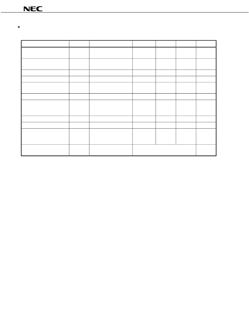
Flash Memory Programming Mode
Write/erase characteristics (T
A
= 10 to 40
°
C, V
DD
= AV
DD
= BV
DD
= 3.0 to 3.6 V, V
SS
= AV
SS
= BV
SS
= 0 V)
Parameter
Symbol
Conditions
MIN.
TYP.
MAX.
Unit
V
PP
supply voltage
V
PP2
During flash memory
programming
7.5
7.8
8.1
V
V
DD
supply current
I
DD
When V
PP
= V
PP2
, f
XX
= 20
MHz
67
mA
V
PP
supply current
I
PP
V
PP
= V
PP2
200
mA
Step erase time
t
ER
Note 1
0.2
s
Overall erase time per area
t
ERA
When the step erase time
= 0.2 s,
Note 2
20
s/area
Write-back time
t
WB
Note 3
1
ms
Number of write-backs per
write-back command
C
WB
When the write-back time
= 1 ms,
Note 4
300
Count/write-
back
command
Number of erase/write-backs
C
ERWB
16
Count
Step writing time
t
WR
Note 5
20
μ
s
Overall writing time per word
t
WRW
When the step writing
time = 20
μ
s (1 word = 4
bytes),
Note 6
20
200
μ
s/word
Number of rewrites per area
C
ERWR
1 erase + 1 write after
erase = 1 rewrite,
Note 7
20
Count/area
Notes 1.
The recommended setting value of the step erase time is 0.2 s.
The prewrite time prior to erasure and the erase verify time (write-back time) are not included.
The recommended setting value of the write-back time is 1 ms.
Write-back is executed once by the issuance of the write-back command. Therefore, the retry count
must be the maximum value minus the number of commands issued.
The recommended setting value of the step writing time is 20
μ
s.
20
μ
s is added to the actual writing time per word. The internal verify time during and after the writing
is not included.
When writing initially to shipped products, it is counted as one rewrite for both
“
erase to write
”
and
“
write only
”
.
Example
(P: Write, E: Erase)
Shipped product
→
P
→
E
→
P
→
E
→
P: 3 rewrites
Shipped product
→
E
→
P
→
E
→
P
→
E
→
P: 3 rewrites
2.
3.
4.
5.
6.
7.
Remarks 1.
When the PG-FP3 is used, a time parameter required for writing/erasing by downloading
parameter files is automatically set. Do not change the settings unless otherwise specified.
2.
Area 0 = 000000H to 01FFFFH (
μ
PD70F3017A, 70F3017AY only)
Area 1 = 020000H to 03FFFFH (
μ
PD70F3017A, 70F3017AY only)
相關(guān)PDF資料 |
PDF描述 |
|---|---|
| UPD72001C-A8 | MULTI-PROTOCOL SERIAL CONTROLLERS |
| UPD72001C | MULTI-PROTOCOL SERIAL CONTROLLERS |
| UPD72001L | MULTI-PROTOCOL SERIAL CONTROLLERS |
| UPD72001GC-11-3B6 | MULTI-PROTOCOL SERIAL CONTROLLERS |
| UPD72001GC-A8-3B6 | MULTI-PROTOCOL SERIAL CONTROLLERS |
相關(guān)代理商/技術(shù)參數(shù) |
參數(shù)描述 |
|---|---|
| uPD70F3017AYGC-8EU(A) | 制造商:Renesas Electronics Corporation 功能描述: |
| UPD70F3017AYGC-8EU-A | 制造商:Renesas Electronics Corporation 功能描述: 制造商:Renesas Electronics Corporation 功能描述:MCU 32-Bit V850 RISC 256KB Flash 3.3V 100-Pin LQFP |
| UPD70F3018GC-7EA-V8 | 制造商:NEC Electronics Corporation 功能描述: |
| UPD70F3025A | 制造商:NEC 制造商全稱:NEC 功能描述:V853TM 32-/16-BIT SINGLE-CHIP MICROCONTROLLER |
| UPD70F3025AGC-25-8EU | 制造商:NEC 制造商全稱:NEC 功能描述:V853TM 32-/16-BIT SINGLE-CHIP MICROCONTROLLER |
發(fā)布緊急采購(gòu),3分鐘左右您將得到回復(fù)。