- 您現(xiàn)在的位置:買賣IC網(wǎng) > PDF目錄383980 > UPD17P135A (NEC Corp.) 4-BIT SINGLE-CHIP MICROCONTROLLER FOR SMALL GENERAL-PURPOSE INFRARED REMOTE CONTROL TRANSMITTER PDF資料下載
參數(shù)資料
| 型號: | UPD17P135A |
| 廠商: | NEC Corp. |
| 元件分類: | 4位微控制器 |
| 英文描述: | 4-BIT SINGLE-CHIP MICROCONTROLLER FOR SMALL GENERAL-PURPOSE INFRARED REMOTE CONTROL TRANSMITTER |
| 中文描述: | 4位單片機的小型通用紅外遙控器 |
| 文件頁數(shù): | 66/292頁 |
| 文件大小: | 754K |
| 代理商: | UPD17P135A |
第1頁第2頁第3頁第4頁第5頁第6頁第7頁第8頁第9頁第10頁第11頁第12頁第13頁第14頁第15頁第16頁第17頁第18頁第19頁第20頁第21頁第22頁第23頁第24頁第25頁第26頁第27頁第28頁第29頁第30頁第31頁第32頁第33頁第34頁第35頁第36頁第37頁第38頁第39頁第40頁第41頁第42頁第43頁第44頁第45頁第46頁第47頁第48頁第49頁第50頁第51頁第52頁第53頁第54頁第55頁第56頁第57頁第58頁第59頁第60頁第61頁第62頁第63頁第64頁第65頁當前第66頁第67頁第68頁第69頁第70頁第71頁第72頁第73頁第74頁第75頁第76頁第77頁第78頁第79頁第80頁第81頁第82頁第83頁第84頁第85頁第86頁第87頁第88頁第89頁第90頁第91頁第92頁第93頁第94頁第95頁第96頁第97頁第98頁第99頁第100頁第101頁第102頁第103頁第104頁第105頁第106頁第107頁第108頁第109頁第110頁第111頁第112頁第113頁第114頁第115頁第116頁第117頁第118頁第119頁第120頁第121頁第122頁第123頁第124頁第125頁第126頁第127頁第128頁第129頁第130頁第131頁第132頁第133頁第134頁第135頁第136頁第137頁第138頁第139頁第140頁第141頁第142頁第143頁第144頁第145頁第146頁第147頁第148頁第149頁第150頁第151頁第152頁第153頁第154頁第155頁第156頁第157頁第158頁第159頁第160頁第161頁第162頁第163頁第164頁第165頁第166頁第167頁第168頁第169頁第170頁第171頁第172頁第173頁第174頁第175頁第176頁第177頁第178頁第179頁第180頁第181頁第182頁第183頁第184頁第185頁第186頁第187頁第188頁第189頁第190頁第191頁第192頁第193頁第194頁第195頁第196頁第197頁第198頁第199頁第200頁第201頁第202頁第203頁第204頁第205頁第206頁第207頁第208頁第209頁第210頁第211頁第212頁第213頁第214頁第215頁第216頁第217頁第218頁第219頁第220頁第221頁第222頁第223頁第224頁第225頁第226頁第227頁第228頁第229頁第230頁第231頁第232頁第233頁第234頁第235頁第236頁第237頁第238頁第239頁第240頁第241頁第242頁第243頁第244頁第245頁第246頁第247頁第248頁第249頁第250頁第251頁第252頁第253頁第254頁第255頁第256頁第257頁第258頁第259頁第260頁第261頁第262頁第263頁第264頁第265頁第266頁第267頁第268頁第269頁第270頁第271頁第272頁第273頁第274頁第275頁第276頁第277頁第278頁第279頁第280頁第281頁第282頁第283頁第284頁第285頁第286頁第287頁第288頁第289頁第290頁第291頁第292頁
CHAPTER 7 SYSTEM REGISTER (SYSREG)
47
7.5 INDEX REGISTER (IX) AND DATA MEMORY ROW ADDRESS POINTER (MEMORY POINTER: MP)
7.5.1 Index Register (IX)
IX is used for address modification of the data memory. The difference between IX and MP is that IX modifies an
address specified by a bank and operand m.
IX is allocated to a total of 12 bits of system register addresses 7AH (IXH), 7BH (IXM), and 7CH (IXL), as shown
in Figure 7-8. Actually, however, only 11 bits, the low-order 3 bits of IXH, IXM, and IXL, function as IX. An index register
enable flag (IXE) which enables address modification by IX is assigned to the least significant bit of PSW.
When IXE = 1, the address of the data memory specified by operand m is not m, but the result of ORing between
m and IXM through IXL. The bank specified at this time is also indicated by ORing BANK and IXH.
Remark
IXH of the
μ
PD17134A subseries is fixed to “0”, and the bank is not modified even when IXE = 1 (to prevent
a bank other than 0 from being used).
7.5.2 Data Memory Row Address Pointer (Memory Pointer: MP)
MP is used for address modification of the data memory. The difference between IX and MP is that MP modifies
the row address of an address indirectly specified by bank and operand @r.
MPH and IXH and MPL and IXM are assigned to the same address (addresses 7AH and 7BH of the system register)
as shown in Figure 7-8. Actually, however, the low-order 3 bits of MPH and MPL, or a total of 7 bits, function as MP.
A memory pointer enable flag (MPE) which enables address modification by MP is assigned to the most significant
bit of MPH.
When MPE = 1, the bank and row address of the data memory indirectly specified by operand @r are not BANK
and m
R
, but the address specified by MP (the column address is specified by the contents of r independently of MPE).
At this time, the low-order 3 bits of MPH and the most significant bit of MPL indicate BANK, and the low-order 3 bits
of MPL indicate a row address.
Remark
The low-order 3 bits of MPH and most significant bit of MPL of the
μ
PD17134A subseries are fixed to
“0”, and bank 0 is always specified even when MPE = 1 (to prevent a bank other than 0 from being used).
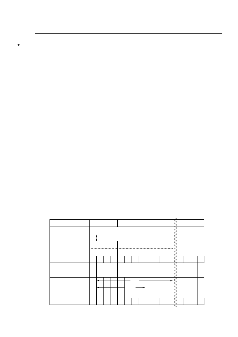
Figure 7-8. Index Register Configuration
0
0
0
0
0
0
0
0
0
0
0
0
0
0
0
7AH
7BH
7CH
7FH
Address
Initial value when reset
0
b
2
b
1
b
0
b
3
b
2
b
1
b
0
b
3
b
2
b
1
b
0
b
3
b
2
b
1
b
3
Index register (IX)
Memory pointer (MP)
IXH
MPH
IXM
MPL
IXL
Bit
Name
Symbolic name
Flag name
Data
0
0
0
(MP)
(IX)
M
P
E
I
X
E
b
0
PSW
0
Low-order 4
bits of program
status word
(PSWORD)
相關PDF資料 |
PDF描述 |
|---|---|
| UPD17P136ACT | 4-BIT SINGLE-CHIP MICROCONTROLLER FOR SMALL GENERAL-PURPOSE INFRARED REMOTE CONTROL TRANSMITTER |
| UPD17P136AGT | 4-BIT SINGLE-CHIP MICROCONTROLLER FOR SMALL GENERAL-PURPOSE INFRARED REMOTE CONTROL TRANSMITTER |
| UPD17P137ACT | 4-BIT SINGLE-CHIP MICROCONTROLLER FOR SMALL GENERAL-PURPOSE INFRARED REMOTE CONTROL TRANSMITTER |
| UPD17P137AGT | 4-BIT SINGLE-CHIP MICROCONTROLLER FOR SMALL GENERAL-PURPOSE INFRARED REMOTE CONTROL TRANSMITTER |
| UPD178P018AGC-3B9 | 8-bit Microcontroller with 2/4/8K Bytes In-System Programmable Flash |
相關代理商/技術參數(shù) |
參數(shù)描述 |
|---|---|
| UPD17P136A | 制造商:未知廠家 制造商全稱:未知廠家 功能描述:UPD17134A Subseries User's Manual | User's Manual[12/1996] |
| UPD17P136ACT | 制造商:NEC 制造商全稱:NEC 功能描述:4-BIT SINGLE-CHIP MICROCONTROLLER |
| UPD17P136AGT | 制造商:NEC 制造商全稱:NEC 功能描述:4-BIT SINGLE-CHIP MICROCONTROLLER |
| UPD17P137A | 制造商:未知廠家 制造商全稱:未知廠家 功能描述:UPD17134A Subseries User's Manual | User's Manual[12/1996] |
| UPD17P137ACT | 制造商:NEC 制造商全稱:NEC 功能描述:4-BIT SINGLE-CHIP MICROCONTROLLER |
發(fā)布緊急采購,3分鐘左右您將得到回復。