- 您現(xiàn)在的位置:買賣IC網(wǎng) > PDF目錄378722 > UCC1888 (Texas Instruments, Inc.) Off-line Power Supply Controller PDF資料下載
參數(shù)資料
| 型號: | UCC1888 |
| 廠商: | Texas Instruments, Inc. |
| 英文描述: | Off-line Power Supply Controller |
| 中文描述: | 脫機(jī)電源控制器 |
| 文件頁數(shù): | 2/6頁 |
| 文件大小: | 299K |
| 代理商: | UCC1888 |
UCC1888
UCC2888
UCC3888
OPERATION (cont.)
At the end of the on time, Q1 is turned off and the current
through R
ON
is again diverted to V
CC
. Thus the current
through R
ON
, which charges C
T
during the on time, con-
tributes to supplying power to the chip during the off time.
The power switch off time is controlled by the discharge
of C
T
which, in turn, is programmed by the regulated out-
put voltage. The relationship between C
T
discharge cur-
rent, I
DCHG
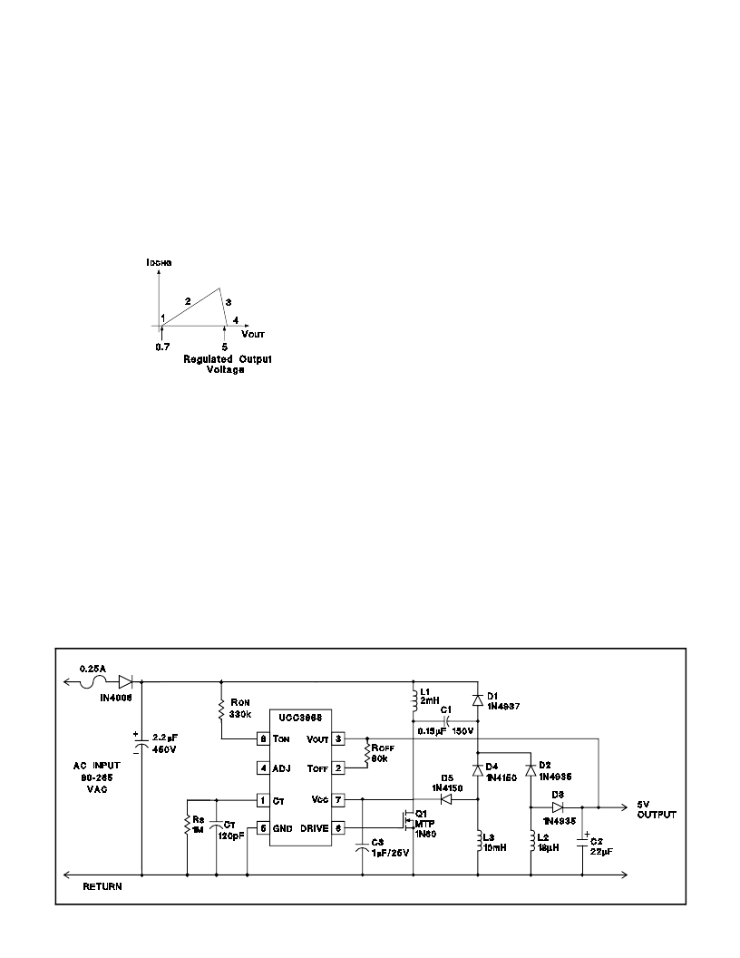
, and output voltage is illustrated as follows:
Region 1. When V
OUT
= 0, the off time is infinite. This
feature provides inherent short circuit protec-
tion. However, to ensure output voltage
startup when the output is not a short, a high
value resistor, R
S
, is placed in parallel with C
T
to establish a minimum switching frequency.
Region 2. As V
OUT
rises above approximately 0.7V to its
regulated value, I
DCHG
is defined by R
OFF
,
and is equal to:
I
DCHG
= (V
OUT
- 0.7V) / R
OFF
As V
OUT
increases, I
DCHG
increases reducing off time.
The operating frequency increases and V
OUT
rises
quickly to its regulated value.
Region 3. In this region, a transconductance amplifier re-
duces I
DCHG
in order to maintain a regulated
V
OUT
.
Region 4. If V
OUT
should rise above its regulation range,
I
DCHG
falls to zero and the circuit returns to
the minimum frequency established by R
S
and
C
T
.
The range of switching frequencies is established by
R
ON
, R
OFF
, R
S
, and C
T
as follows:
Frequency = 1/(T
ON
+ T
OFF
)
T
ON
= R
ON
C
T
4.6
V/(V
IN
- 4.5V)
T
OFF
(max) = 1.4
R
S
C
T
Regions 1 and 4
T
OFF
= R
OFF
C
T
3.7V /(V
OUT
- 0.7V)
Region 2, excluding the effects of R
S
which have a minimal impact on T
OFF
.
The above equations assume that V
CC
equals 9V. The
voltage at T
ON
increases from approximately 2.5V to
6.5V while C
T
is charging. To take this into account, V
IN
is adjusted by 4.5V in the calculation of T
ON
. The voltage
at T
OFF
is approximately 0.7V.
DESIGN EXAMPLE
The UCC3888 regulates a 5 volt, 1 Watt nonisolated DC output from AC inputs between 80 and 265 volts. In this ex-
ample, the IC is programmed to deliver a maximum on time gate drive pulse width of 2.2 microseconds which occurs
at 80 VAC. The corresponding switching frequency is approximately 100kHz at low line, and overall efficiency is ap-
proximately 50%. Additional design information is available in Unitrode Application Note U-149.
UDG-96014
2
相關(guān)PDF資料 |
PDF描述 |
|---|---|
| UCC2888 | Off-line Power Supply Controller |
| UCC1926 | 【 20A Integrated Current Sensor |
| UCC2807PWTR-3 | Programmable Maximum Duty Cycle PWM Controller |
| UCC2807PW-3 | Programmable Maximum Duty Cycle PWM Controller |
| UCC2895QTR | BiCMOS Advanced Phase Shift PWM Controller |
相關(guān)代理商/技術(shù)參數(shù) |
參數(shù)描述 |
|---|---|
| UCC1888J | 制造商:Texas Instruments 功能描述:- Rail/Tube |
| UCC1889 | 制造商:TI 制造商全稱:Texas Instruments 功能描述:Off-line Power Supply Controller |
| UCC1889J | 制造商:未知廠家 制造商全稱:未知廠家 功能描述:Voltage-Mode SMPS Controller |
| UCC1890 | 制造商:TI 制造商全稱:Texas Instruments 功能描述:Off-Line Battery Charger Circuit |
| UCC1895 | 制造商:TI 制造商全稱:Texas Instruments 功能描述:BiCMOS ADVANCED PHASE-SHIFT PWM CONTROLLER |
發(fā)布緊急采購,3分鐘左右您將得到回復(fù)。