- 您現(xiàn)在的位置:買賣IC網(wǎng) > PDF目錄378722 > UCC1837 (Texas Instruments, Inc.) RSO-S_D(Z) Series - Econoline Regulated DC-DC Converters; Input Voltage (Vdc): 12V; Output Voltage (Vdc): 05V; Power: 1W; 2:1 and 4:1 Wide Input Voltage Ranges; 1kVDC, 2kVD & 3kVDC Isolation; UL94V-0 Package Material; Continuous Short Circuit Protectionwith Current Foldback; Low Noise; No External Capacitor needed; Efficiency to 83% PDF資料下載
參數(shù)資料
| 型號: | UCC1837 |
| 廠商: | Texas Instruments, Inc. |
| 元件分類: | DC/DC變換器 |
| 英文描述: | RSO-S_D(Z) Series - Econoline Regulated DC-DC Converters; Input Voltage (Vdc): 12V; Output Voltage (Vdc): 05V; Power: 1W; 2:1 and 4:1 Wide Input Voltage Ranges; 1kVDC, 2kVD & 3kVDC Isolation; UL94V-0 Package Material; Continuous Short Circuit Protectionwith Current Foldback; Low Noise; No External Capacitor needed; Efficiency to 83% |
| 中文描述: | 8引腳? - FET的線性穩(wěn)壓器控制器 |
| 文件頁數(shù): | 4/8頁 |
| 文件大小: | 87K |
| 代理商: | UCC1837 |
4
UCC1837
UCC2837
UCC3837
of the CAP voltage should the external load exceed the
average current, which occurs during load and line tran-
sient conditions. The value of CAP also determines the
startup time of the linear regulator. The voltage at CAP
charges up with a time constant determined by the
charge pump output impedance (typically 80k
) and the
value of the capacitor on CAP.
An external voltage such as +12V may be tied to the
CAP pin directly to insure a higher value of VOUT, which
may be useful when a standard level MOSFET is used or
when VDD is very low and the resulting VOUT voltage
may need to be higher. With an external source applied
to CAP, the maximum voltage at VOUT will be approxi-
mately 1V below the external source.The external +12V
source should be decoupled to GND using a minimum of
a 0.01
μ
F capacitor.
Choosing a Pass Element
The UCC3837 is designed for use with an N-channel
MOSFET pass element only. The designer may choose
a logic level or standard gate level MOSFET depending
on the input voltage, the required gate drive, and the
available voltage at VOUT as discussed previously.
MOSFET selection should be based on required dropout
voltage and gate drive characteristics. A lower R
DS(on)
MOSFET is used when low dropout is required, but this
type of MOSFET will have higher gate capacitance which
may result in a slower transient response.
A MOSFET used in linear regulation is typically operated
at a gate voltage between the threshold voltage and the
gate plateau voltage in order to maintain high gain. This
mode of operation is linear, and therefore the channel re-
sistance is higher than the manufacturer’s published
R
DS(on)
value. The MOSFET should only be operated in
the non-linear (switch) mode under transient conditions,
when minimum dropout voltage is required.
Disabling the UCC3837
Grounding the CAP pin will remove the drive voltage and
effectively disable the output voltage. The device used to
short the output of CAP should have a very low leakage
current when in the OPEN state, since even a few
microamps will lower the charge pump voltage.
A second method of disabling the UCC3837 is to place a
short circuit across C
COMP
. This will have an advantage
of a quicker restart time as the voltage at CAP will not be
completely discharged. The charge pump will be loaded
down by the typical 40
μ
A charging current of the error
amplifier with this configuration, resulting in a lower volt-
age at CAP.
Compensating the Error Amplifier
Using a MOSFET as an external pass element intro-
duces a pole in the control loop that is a function of the
UCC3837 output impedance, R
OUT
, typically 6.5k
, and
the MOSFET input gate capacitance. Fig. 3 indicates
that in the normal operation of a linear regulator using a
MOSFET, the gate capacitance can be predicted directly
from the MOSFET characteristic charge curve, using the
relationship:
Qgth
Vgth
C
IN
=
This pole can be canceled by programming a zero fre-
quency on the output of the UCC3837 error amplifier
equal to the pole frequency. Therefore:
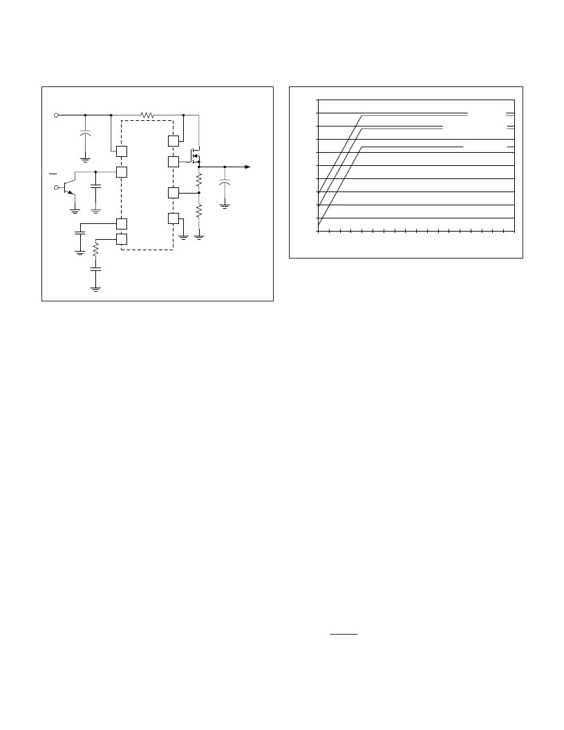
8
1
VDD
CS
5
VOUT
2
CAP
7
CT
4
COMP
6
FB
3
GND
Q1
IRL2203N
OR EQUIVALENT
R2
1.8k
R3
1.5k
C3
1000
μ
F
3.3V
R1
0.020
R
COMP
C
820pF
0.1
μ
F
0.1
μ
F
Q1
C1
330
μ
F
5V
ON/OFF
UCC3837
Figure 1. Typical application 5V to 3.3V, 5A
APPLICATION INFORMATION
5
6
7
8
9
10
11
12
13
14
15
3
4
5
6
7
8
9
10
11
12
VDD
V
E/A DISABLED
LINEAR REGULATOR
OVERDRIVE
Figure 2. Typical V
OUT(max)
vs. VDD.
UDG-99137
相關(guān)PDF資料 |
PDF描述 |
|---|---|
| UCC1839 | RSO-S_D(Z) Series - Econoline Regulated DC-DC Converters; Input Voltage (Vdc): 12V; Output Voltage (Vdc): 05V; Power: 1W; 2:1 and 4:1 Wide Input Voltage Ranges; 1kVDC, 2kVD & 3kVDC Isolation; UL94V-0 Package Material; Continuous Short Circuit Protectionwith Current Foldback; Low Noise; No External Capacitor needed; Efficiency to 83% |
| UCC18500 | BiCMOS PFC/PWM Combination Controller |
| UCC18502 | BiCMOS PFC/PWM Combination Controller |
| UCC18503 | BiCMOS PFC/PWM Combination Controller |
| UCC28502 | BiCMOS PFC/PWM Combination Controller |
相關(guān)代理商/技術(shù)參數(shù) |
參數(shù)描述 |
|---|---|
| UCC1839 | 制造商:TI 制造商全稱:Texas Instruments 功能描述:Secondary Side Average Current Mode Controller |
| UCC1839J | 制造商:未知廠家 制造商全稱:未知廠家 功能描述:Current/Voltage-Mode SMPS Controller |
| UCC18500 | 制造商:TI 制造商全稱:Texas Instruments 功能描述:BiCMOS PFC/PWM Combination Controller |
| UCC18501 | 制造商:TI 制造商全稱:Texas Instruments 功能描述:BiCMOS PFC/PWM Combination Controller |
| UCC18502 | 制造商:TI 制造商全稱:Texas Instruments 功能描述:BiCMOS PFC/PWM Combination Controller |
發(fā)布緊急采購,3分鐘左右您將得到回復(fù)。