- 您現(xiàn)在的位置:買賣IC網(wǎng) > PDF目錄378722 > UC3175 (Texas Instruments, Inc.) Full-Bridge Power Amplifier PDF資料下載
參數(shù)資料
| 型號: | UC3175 |
| 廠商: | Texas Instruments, Inc. |
| 英文描述: | Full-Bridge Power Amplifier |
| 中文描述: | 全橋功率放大器 |
| 文件頁數(shù): | 2/6頁 |
| 文件大?。?/td> | 343K |
| 代理商: | UC3175 |
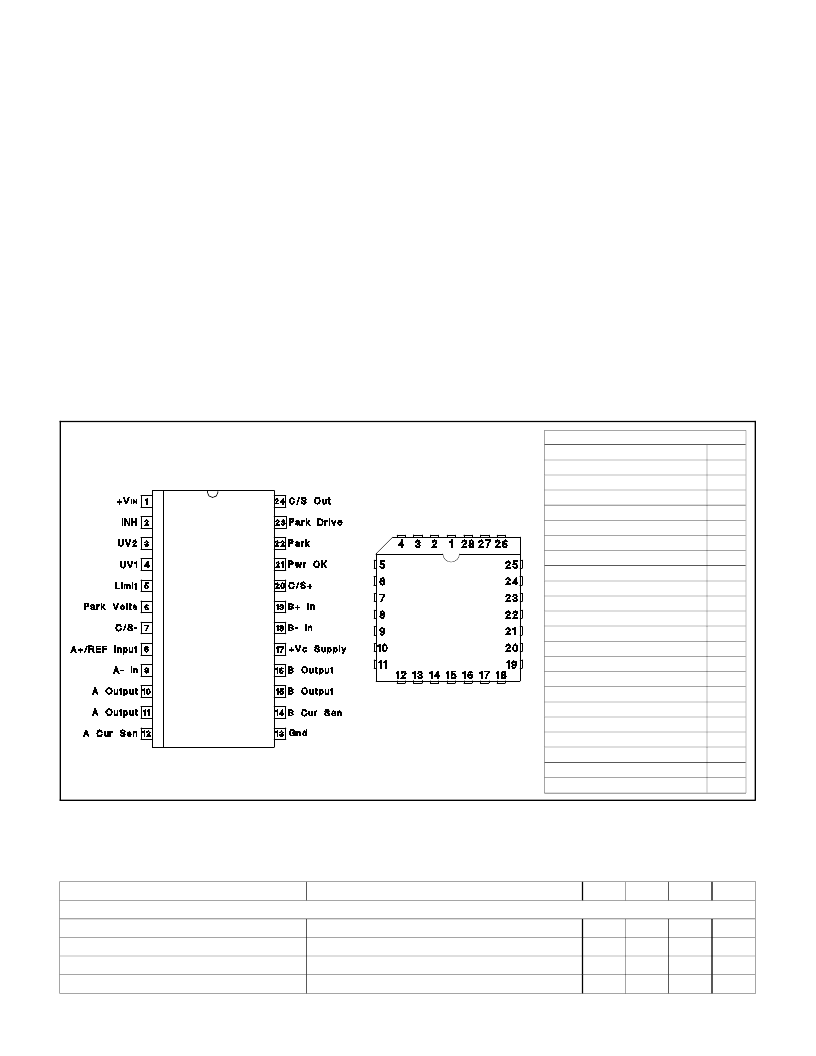
CONNECTION DIAGRAMS
UC3175B
PACKAGE PIN FUNCTION
FUNCTION
+V
IN
INH
UV2
UV1
Limit
Park Volts
C/S-
A+/REF Input
A- In
A Output
A Cur Sen
Gnd (Heat Dissipation Pins) 12-18
B Cur Sen
B Output
+V
C
Supply
B- In
B+ In
C/S+
Pwr OK
Park
Park Drive
C/S Out
PIN
1
2
3
4
5
6
7
8
9
10
11
19
20
21
22
23
24
25
26
27
28
PLCC-28 (Top View)
QP Package
ABSOLUTE MAXIMUM RATINGS
Input Supply Voltage, (+V
IN
,+V
C
). . . . . . . . . . . . . . . . . . . . . . . . . . . . . . . . 20V
UV Comparator, and Digital Inputs
Maximum forced voltage. . . . . . . . . . . . . . . . . . . . . . . . . . . . . -0.3V to 10V
Maximum forced current . . . . . . . . . . . . . . . . . . . . . . . . . . . . . . . . .
±
10mA
C/S Inputs
Maximum forced voltage. . . . . . . . . . . . . . . . . . . . . . . . . . . . . -0.3V to 20V
A and B Amplifier Inputs . . . . . . . . . . . . . . . . . . . . . . . . . . . . -0.3V to +V
IN
Open Collector Output Voltages. . . . . . . . . . . . . . . . . . . . . . . . . . . . . . . . . 20V
A and B Output Currents (continuous)
Source . . . . . . . . . . . . . . . . . . . . . . . . . . . . . . . . . . . . . . . Internally Limited
Sink . . . . . . . . . . . . . . . . . . . . . . . . . . . . . . . . . . . . . . . . . . . . . . . . . . . 1.0A
Parking Drive Output Current
Continuous . . . . . . . . . . . . . . . . . . . . . . . . . . . . . . . . . . . . . . . . . . . 150mA
Pulsed . . . . . . . . . . . . . . . . . . . . . . . . . . . . . . . . . . . . . . . . . . . . . . . . . . . 1A
Output Diode Current (pulsed). . . . . . . . . . . . . . . . . . . . . . . . . . . . . . . . . . . 1A
Power OK Output Current(continuous) . . . . . . . . . . . . . . . . . . . . . . . . . 30mA
Operating Junction Temperature . . . . . . . . . . . . . . . . . . . . . . -55
°
C to +150
°
C
Storage Temperature . . . . . . . . . . . . . . . . . . . . . . . . . . . . . . . -65
°
C to +150
°
C
Note 1: Unless otherwise indicated, voltages are
referenced to ground and currents are positive
into, negative out of, the specified terminals.
"Pulsed" is defined as a less than 10% duty cycle
pulse with a maximum duration of 500
μ
s.
Note 2: See Unitrode Integrated Circuits databook
for information regarding thermal specifications
and limitations of packages.
PARAMETER
TEST CONDITIONS
MIN
TYP
MAX
UNITS
INPUT SUPPLY
+V
IN
Supply Current
+V
C
Supply Current
+V
IN
UVLO Threshold
UVLO Threshold Hysteresis
All Amplifier Outputs = 6V
I
OUT
= 0A
Low to High
35
1
2.8
200
42
mA
mA
V
mV
3.0
ELECTRICAL CHARACTERISTICS:
Unless otherwise stated specifications apply for 0
°
C
≤
T
A
≤
70
°
C, +V
IN
= 12V, +V
C
= +V
IN
, A+/REF Input = 6V. T
A
=T
J
.
SOIC-24 (Top View)
DW Package
Thermal Data
QP Package:
Thermal Resistance Junction to Leads,
θ
JL
. . . . . . . . . . . . . . . . . . . . . . . 15
°
C/W
Thermal Resistance Junction to Ambient,
θ
JA
. . . . . . . . . . . . . . . . . . . . . . . 40
°
C/W
2
相關(guān)PDF資料 |
PDF描述 |
|---|---|
| UC3175B | Full-Bridge Power Amplifier |
| UC494 | Advanced Regulating Pulse Width Modulators |
| UC495ACJ | Very low drop voltage regulators with inhibit |
| UC495AJ | Very low drop voltage regulators with inhibit |
| UC495AN | Very low drop voltage regulators with inhibit |
相關(guān)代理商/技術(shù)參數(shù) |
參數(shù)描述 |
|---|---|
| UC3175B | 制造商:TI 制造商全稱:Texas Instruments 功能描述:Full-Bridge Power Amplifier |
| UC3175BDW | 制造商:未知廠家 制造商全稱:未知廠家 功能描述:Servo Motor Controller/Driver |
| UC3175BDWTR | 制造商:未知廠家 制造商全稱:未知廠家 功能描述:Servo Motor Controller/Driver |
| UC3175BQP | 制造商:未知廠家 制造商全稱:未知廠家 功能描述:Servo Motor Controller/Driver |
| UC3175BQPTR | 制造商:未知廠家 制造商全稱:未知廠家 功能描述:Servo Motor Controller/Driver |
發(fā)布緊急采購,3分鐘左右您將得到回復(fù)。