- 您現(xiàn)在的位置:買賣IC網(wǎng) > PDF目錄378722 > UC2854BQTR (Texas Instruments, Inc.) Power Factor Controller PDF資料下載
參數(shù)資料
| 型號(hào): | UC2854BQTR |
| 廠商: | Texas Instruments, Inc. |
| 元件分類: | 基準(zhǔn)電壓源/電流源 |
| 英文描述: | Power Factor Controller |
| 中文描述: | 功率因數(shù)控制器 |
| 文件頁數(shù): | 6/16頁 |
| 文件大?。?/td> | 455K |
| 代理商: | UC2854BQTR |
SLUS329B JUNE 1998 REVISED FEBRUARY 2005
6
www.ti.com
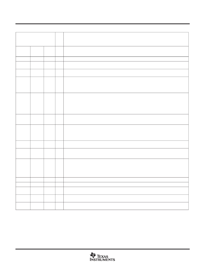
TERMINAL FUNCTIONS
TERMINAL
PACKAGES
NAME
I/O
DESCRIPTION
J/N/DW
Q/L
CAO
3
4
O
Output of the wide bandwidth current amplifier and one of the inputs to the PWM duty-cycle
comparator. The output signal generated by this amplifier commands the PWM to force the correct
input current. The output can swing from 0.1 V to 7.5 V.
CT
14
18
I
Capacitor from CT to GND sets the PWM oscillator frequency
ENA
10
13
I
A nominal voltage above 2.65 V on this pin allows the device to begin operating. Once operating,
the device shuts off if this pin goes below 2.15 V nominal.
GND
1
2
All bypass and timing capacitors connected to GND should have leads as short and direct as
possible. All voltages are measured with respect GND.
GTDRV
16
20
O
Output of the PWM is a 1.5-A peak totem-pole MOSFET gate driver on GTDRV. This output is
internally clamped to 15 V so that the device can be operated with VCC as high as 35 V. Use a
series gate resistor of at least 5
to prevent interaction between the gate impedance and the
GTDRV output driver that might cause the GTDRV output to overshoot excessively. Some
overshoot of the GTDRV output is always expected when driving a capacitive load.
IAC
6
8
I
Current input to the multiplier, proportional to the instantaneous line voltage. This input to the
analog multiplier is a current. The multiplier is tailored for very low distortion from this current input
(IAC) to MOUT, so this is the only multiplier input that should be used for sensing instantaneous
line voltage. The nominal voltage on IAC is 6 V, so in addition to a resistor from IAC to rectified
60 Hz, connect a resistor from IAC to VREF. If the resistor to VREF is one-fourth of the value of the
resistor to the rectifier, then the 6-V offset is cancelled, and the line current has minimal cross-over
distortion.
ISENSE
4
5
I
Switch current sensing input. This is the inverting input to the current amplifier. This input and the
non-inverting input MOUT remain functional down to and below GND. Care should be taken to
avoid taking these inputs below 0.5V, because they are protected with diodes to GND.
MOUT
5
7
I/O
Multiplier output and current sense plus. The output of the analog multiplier and the non-inverting
input of the current amplifier are connected together at MOUT. The cautions about taking ISENSE
below 0.5V also apply to MOUT. As the multiplier output is a current, this is a high-impedance
input similar to ISENSE, so the current amplifier can be configured as a differential amplifier to reject
PKLMT
2
3
I
Peak limit. The threshold for PKLMT is 0.0 V. Connect this input to the negative voltage on the
current sense resistor. Use a resistor to REF to offset the negative current sense signal up to GND.
RSET
12
15
I
Oscillator charging current and multiplier limit set. A resistor from RSET to ground programs
oscillator charging current. Multiplier output current does not exceed 3.75V divided by the resistor
from RSET to ground.
SS
13
17
I
Soft-start. SS remains at GND as long as the device is disabled or VCC is too low. SS pulls up to
over 8 V by an internal 14-mA current source when both VCC becomes valid and the device is
enabled. SS acts as the reference input to the voltage amplifier if SS is below VREF. With a large
capacitor from SS to GND, the reference to the voltage regulating amplifier rises slowly, and
increase the PWM duty cycle slowly. In the event of a disable command or a supply dropout, SS
will quickly discharge to ground and disable the PWM.
VAO
7
9
I
Voltage amplifier output
VCC
15
19
I
Positive supply rail
VREF
9
12
O
Used to set the peak limit point and as an internal reference for various device functions. This
voltage must be present for the device to operate.
VRMS
8
10
I
One of the inputs into the multiplier. This pin provides the input RMS voltage to the multiplier
circuitry.
VSENSE
11
14
I
This pin provides the feedback from the output. This input goes into the voltage error amplifier and
the output of the error amplifier is another of the inputs into the multiplier circuit.
相關(guān)PDF資料 |
PDF描述 |
|---|---|
| UC3175 | Full-Bridge Power Amplifier |
| UC3175B | Full-Bridge Power Amplifier |
| UC494 | Advanced Regulating Pulse Width Modulators |
| UC495ACJ | Very low drop voltage regulators with inhibit |
| UC495AJ | Very low drop voltage regulators with inhibit |
相關(guān)代理商/技術(shù)參數(shù) |
參數(shù)描述 |
|---|---|
| UC2854DW | 功能描述:功率因數(shù)校正 IC High Power-Factor Preregulator RoHS:否 制造商:Fairchild Semiconductor 開關(guān)頻率:300 KHz 最大功率耗散: 最大工作溫度:+ 125 C 安裝風(fēng)格:SMD/SMT 封裝 / 箱體:SOIC-8 封裝:Reel |
| UC2854DWG4 | 功能描述:功率因數(shù)校正 IC High Power-Factor Preregulator RoHS:否 制造商:Fairchild Semiconductor 開關(guān)頻率:300 KHz 最大功率耗散: 最大工作溫度:+ 125 C 安裝風(fēng)格:SMD/SMT 封裝 / 箱體:SOIC-8 封裝:Reel |
| UC2854DWTR | 功能描述:功率因數(shù)校正 IC HP Factor Pre-Reg RoHS:否 制造商:Fairchild Semiconductor 開關(guān)頻率:300 KHz 最大功率耗散: 最大工作溫度:+ 125 C 安裝風(fēng)格:SMD/SMT 封裝 / 箱體:SOIC-8 封裝:Reel |
| UC2854DWTRG4 | 功能描述:功率因數(shù)校正 IC High Power-Factor Preregulator RoHS:否 制造商:Fairchild Semiconductor 開關(guān)頻率:300 KHz 最大功率耗散: 最大工作溫度:+ 125 C 安裝風(fēng)格:SMD/SMT 封裝 / 箱體:SOIC-8 封裝:Reel |
| UC2854J | 制造商:Texas Instruments 功能描述:Power Factor Correction PREREGUL 1.5mA 118KHz 16-Pin CDIP 制造商:Texas Instruments 功能描述:PWR FCTR CORRECTION PREREGUL 1.5MA 118KHZ 16CDIP - Rail/Tube |
發(fā)布緊急采購,3分鐘左右您將得到回復(fù)。