- 您現(xiàn)在的位置:買賣IC網(wǎng) > PDF目錄378721 > UC1844A (Microsemi Corporation) CURRENT MODE PWM CONTROLLER PDF資料下載
參數(shù)資料
| 型號(hào): | UC1844A |
| 廠商: | Microsemi Corporation |
| 英文描述: | CURRENT MODE PWM CONTROLLER |
| 中文描述: | 電流模式PWM控制器 |
| 文件頁數(shù): | 4/11頁 |
| 文件大小: | 661K |
| 代理商: | UC1844A |
4
UC1842A/3A/4A/5A
UC2842A/3A/4A/5A
UC3842A/3A/4A/5A
PARAMETER
TEST CONDITIONS
UC184xA\UC284xA
MIN.
TYP.
UC384xA
TYP.
UNITS
MAX.
MIN.
MAX.
Under-Voltage Lockout Section
Start Threshold
x842A/4A
x843A/5A
x842A/4A
x843A/5A
15
7.8
9
7.0
16
8.4
10
7.6
17
9.0
11
8.2
14.5
7.8
8.5
7.0
16
8.4
10
7.6
17.5
9.0
11.5
8.2
V
V
V
V
Min. Operation Voltage After
Turn On
PWM Section
Maximum Duty Cycle
x842A/3A
x844A/5A
94
47
96
48
100
50
0
94
47
96
48
100
50
0
%
%
%
Minimum Duty Cycle
Total Standby Current
Start-Up Current
Operating Supply Current
V
CC
Zener Voltage
0.3
11
34
0.5
17
0.3
11
34
0.5
17
mA
mA
V
V
PIN 2
= V
PIN 3
= 0V
I
CC
= 25mA
30
30
Note 2:
Ensured by design, but not 100% production tested.
Note 3:
Parameter measured at trip point of latch with V
PIN2
= 0.
Note 4:
Gain defined as: A
VPIN
Note 5:
Adjust V
CC
above the start threshold before setting at 15V
Note 6:
Output frequency equals oscillator frequency for the UC1842A and UC1843A. Output frequency is one half oscillator fre-
quency for the UC1844A and UC1845A.
Note 7:
“Temperature stability, sometimes referred to as average temperature coefficient, is described by the equation:
TempStability
TJ max
TJ min
(
)
(
)
age measured over the appropriate temperature range. Note that the extremes in voltage do not necessarily occur at the extremes
in temperature.”
Note 8:
This parameter is measured with R
T
= 10k
to V
REF
.This contributes approximately 300 A of current to the measurement.
The total current flowing into the R
T
/C
pin will be approximately 300
A higher than the measured value.
VPIN
=
1
3; 0
V
PIN 3
0.8V
VREF max
VREF min
=
(
)
(
)
.V
REF
(max) and V
REF
(min) are the maximum & minimum reference volt-
ELECTRICAL CHARACTERISTICS
Unless otherwise stated, these specifications apply for –55
°
C
≤
T
A
≤
125°C for the
UC184xA; –40
°
C
≤
T
A
≤
125°C for the UC284xAQ; –40
°
C
≤
T
A
≤
85
°
C for the UC284xA; 0
≤
T
A
≤
70
°
C for the UC384xA; V
CC
= 15V
(Note 5); R
T
= 10k; C
T
= 3.3nF; T
A
= T
J
; Pin numbers refer to DIL-8.
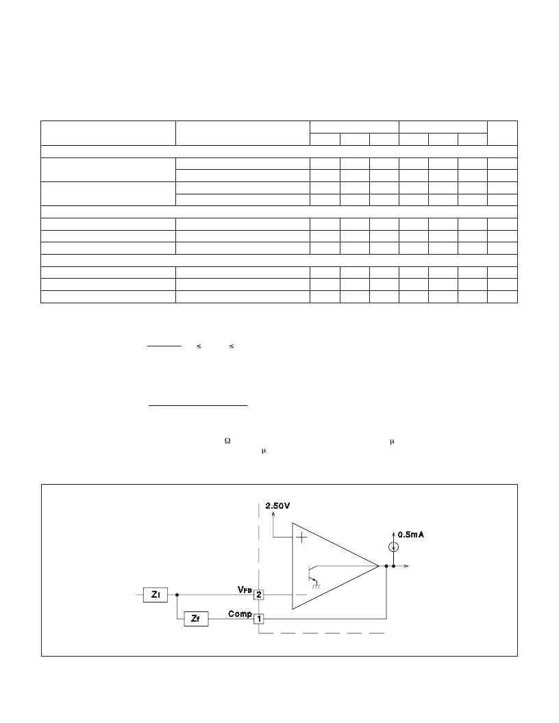
Error Amp Configuration
Error Amp can Source and Sink up to 0.5mA, and Sink up to 2mA.
相關(guān)PDF資料 |
PDF描述 |
|---|---|
| UC1843A | CURRENT MODE PWM CONTROLLER |
| UC1844AY | Single chip RDS demodulator |
| UC1874DW-1 | High Efficiency, Synchronous, Step-down Buck Controllers |
| UC1874DW-2 | High Efficiency, Synchronous, Step-down Buck Controllers |
| UC1874J-1 | High Efficiency, Synchronous, Step-down Buck Controllers |
相關(guān)代理商/技術(shù)參數(shù) |
參數(shù)描述 |
|---|---|
| UC1844A DIE | 制造商:Texas Instruments 功能描述: |
| UC1844AAY | 制造商:MICROSEMI 制造商全稱:Microsemi Corporation 功能描述:CURRENT MODE PWM CONTROLLER |
| UC1844A-EP | 制造商:TI 制造商全稱:Texas Instruments 功能描述:CURRENT-MODE PWM CONTROLLER |
| UC1844AJ | 制造商:Texas Instruments 功能描述:Current Mode PWM Controller 1A 8-Pin CDIP Tube 制造商:Rochester Electronics LLC 功能描述:CUR MODE PWM CONT - Bulk |
| UC1844AJ/90027 | 制造商:Rochester Electronics LLC 功能描述:- Bulk |
發(fā)布緊急采購,3分鐘左右您將得到回復(fù)。