- 您現(xiàn)在的位置:買賣IC網(wǎng) > PDF目錄382702 > U2320B VHF/UHF Tuner-IC PDF資料下載
參數(shù)資料
| 型號(hào): | U2320B |
| 英文描述: | VHF/UHF Tuner-IC |
| 中文描述: | 甚高頻/超高頻調(diào)諧器集成電路 |
| 文件頁數(shù): | 3/7頁 |
| 文件大小: | 159K |
| 代理商: | U2320B |

U2320B
TELEFUNKEN Semiconductors
Rev. A1, 29-May-96
3 (7)
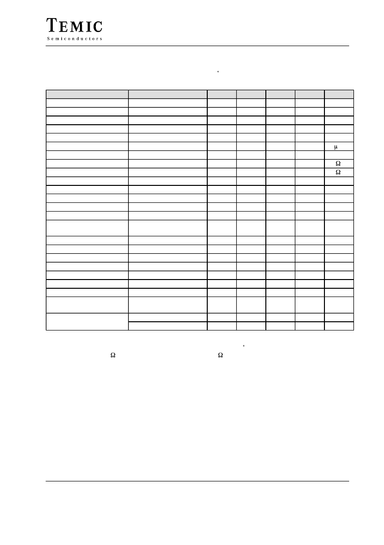
Electrical Characteristics
Test conditions (unless otherwise specified): Vs = 12 V, T
amb
= 25 C,
reference point Pin 2, referred to test circuit page 5.
Parameters
Test Conditions / Pins
Symbol
V
S
I
S
Min.
10.8
Typ.
12.0
42
Max.
13.2
50
Unit
V
mA
Supply voltage
Supply current
Band switch
Voltage band A
Voltage band B
Switching current
SAW filter driver
Input impedance
Output impedance
Voltage gain
Band A (note 1)
Input frequency range
Input impedance
Gain (note 4)
Noise figure DSB (note 2)
Pin 13-15
Pin 13-15
Pin 8
Pin 8
Pin 8
VSWA
VSWB
ISW
0
0
1.0
5.0
100
V
V
A
3.4
4.0
VSW = 5 V
fi = 36 MHz
Pin 11, 12
Pin 9, 10
ZiSAW
ZoSAW
GvSAW
450
70
19
11, 12
→
9, 10
dB
Pin18
Pin18
I/P to O/P
I/P to O/P
fiA
S11A
GA
NF
48
470
MHz
Figure 4
30
11.5
12
dB
dB
dB
fiA = 50 MHz
fiA = 150 MHz
Each carrier
fiA = 71 MHz
fiA = 71 MHz
Input level for (note 3):
IM3 (Interm. of 3rd order)
IM2 (Interm. of 2nd order)
Band B (note 1)
Input frequency range
Input impedance
Gain (note 4)
Noise figure DSB (note 2)
I/P
I/P
ViA
ViA
–22
–22
dBm
dBm
Pin 16, 17
Pin 16, 17
I/P to O/P
I/P to O/P
fiB
S11B
GB
NF
470
860
MHz
Figure 4
34
10.5
11.5
dB
dB
dB
fiB = 500 MHz
fiB = 800 MHz
Each carrier
fiB = 600 MHz
Input level for IM3
(Interm. of 3rd order, note 3)
I/P
ViB
–27
dBm
Notes
1)
The RF input B is symmetrical driven by means of a hybrid for 180 phase shifting, consequently the source
impedance is 100 . All other impedance for RF tests is 50 .
The noise figure (NF) is the value for double-side-band measurement.
The intermodulation test (2-carrier-method) which is made on IF-centre
is in reference to a signal-to-IM ratio of 60 dB.
Gain is the ratio of the voltage at the primary coil of L5 to the available voltage at the input.
2)
3)
4
)
相關(guān)PDF資料 |
PDF描述 |
|---|---|
| U2320B-FLG3 | VHF/UHF Tuner-IC |
| U2350B | PWM Speed Control for Permanent Excited DC Motors |
| U2350B-FP | PWM Speed Control for Permanent Excited DC Motors |
| U2352 | PWM Power Control for DC Loads |
| U2352B | PWM Power Control for DC Loads |
相關(guān)代理商/技術(shù)參數(shù) |
參數(shù)描述 |
|---|---|
| U2320B-FLG3 | 制造商:TEMIC 制造商全稱:TEMIC Semiconductors 功能描述:VHF/UHF Tuner-IC |
| U2-321 | 制造商:OTTO Engineering Inc 功能描述:B3-31141 AND |
| U2-322 | 制造商:OTTO Engineering Inc 功能描述:THREE POSITION WITH |
| U2-323 | 制造商:OTTO Engineering Inc 功能描述:U2-016 EX. W/ GRAY |
| U2-324 | 制造商:OTTO Engineering Inc 功能描述:LH GRIP, S/A U2-149 |
發(fā)布緊急采購,3分鐘左右您將得到回復(fù)。