- 您現(xiàn)在的位置:買賣IC網(wǎng) > PDF目錄382702 > U210B-FP Phase Control Circuit - Load Current Feedback Applications PDF資料下載
參數(shù)資料
| 型號: | U210B-FP |
| 英文描述: | Phase Control Circuit - Load Current Feedback Applications |
| 中文描述: | 相位控制電路-負(fù)載電流反饋的應(yīng)用 |
| 文件頁數(shù): | 3/15頁 |
| 文件大?。?/td> | 378K |
| 代理商: | U210B-FP |

TELEFUNKEN Semiconductors
U 210 B / U 210 B–FP
3
Preliminary Information
Description
Mains supply
The U 210 B is fitted with voltage limiting and can therefore be supplied directly from the mains. The supply voltage
between Pin 2 (+pol/
) and Pin 3 builds up across D
1
and R
1
and is smoothed by C
1
. The vaIue of the series resistance
can be approximated using:
V
M
–V
S
R
1
=
2 I
S
Further information regarding the design of the mains supply can be found in the data sheets in the appendix. The reference
voltage source on Pin 13 of typ. –8.9 V is derived from the supply voltage. It represents the reference level of the control
unit. Operating using an externally stabiIised DC voltage is not recommended.
If the supply cannot be taken directly from the mains because the power dissipation in R
1
would be too large, then the
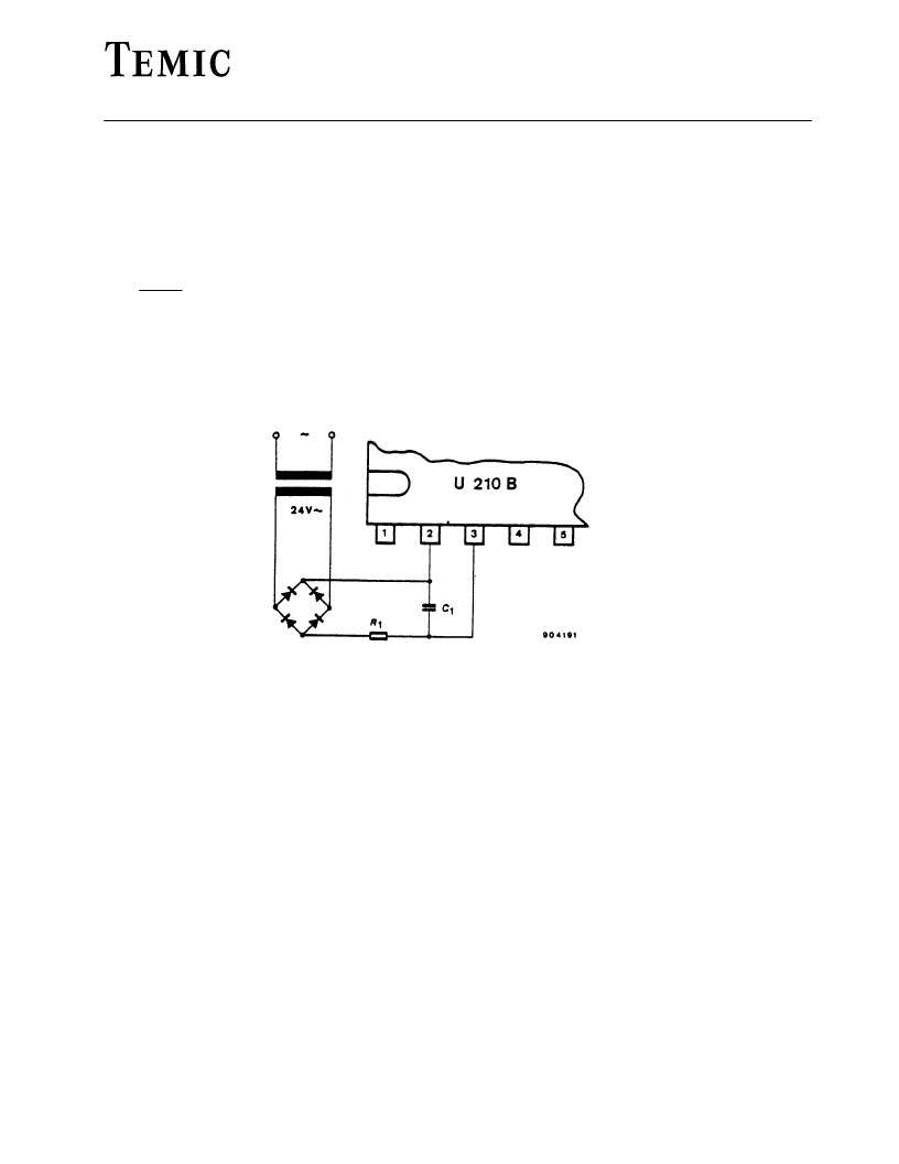
circuit shown in the following Figure 3 should be employed.
Figure 3 Supply voltage for high current requirements
Phase control
The function of the phase control is largely identical to that of the well known components U 111 B and TEA 1007. The
phase angle of the trigger pulse is derived by comparing the ramp voltage, which is mains synchronised by the voltage
detector, with the set value on the control input Pin 9. The slope of the ramp is determined by C
2
and its charging current.
The charging current can be varied using R
2
on Pin 5. The maximum phase angle
max
can also be adjusted using R
2
.
When the potential on Pin 6 reaches the nominal value predetermined at Pin 9, then a trigger pulse is generated whose
width t
p
is determined by the value of C
2
(the value of C
2
and hence the pulse width can be evaluated by assuming 8 s/nF).
At the same time, a latch is set, so that as long as the automatic retriggering has not been activated, then no more pulses
can be generated in that half cycle.
The current sensor on Pin 1 ensures that, for operation with inductive loads, no pulse will be generated in a new half cycle
as long as current from the previous half cycle is still flowing in the opposite direction to the supply voltage at that instant.
This makes sure that ”Gaps” in the load current are prevented.
The control signal on Pin 9 can be in the range 0 V to –7 V (reference point Pin 2).
If V
pin9
= –7 V then the phase angle is at maximum =
max
i .e. the current flow angle is a minimum. The minimum phase
angle
min
is when V
pin9
= V
pin2
.
Voltage monitoring
As the voltage is built up, uncontrolled output pulses are avoided by internal voltage surveillance. At the same time, all
of the latches in the circuit (phase control, soft start) are reset and the soft–start capacitor is short circuited. Used with
a switching hysteresis of 300 mV, this system guarantees defined start–up behaviour each time the supply voltage is
switched on or after short interruptions of the mains supply.
相關(guān)PDF資料 |
PDF描述 |
|---|---|
| U211B | Phase Control Circuit - General Purpose Feedback |
| U211B2 | Phase Control Circuit - General Purpose Feedback |
| U211B3 | Phase Control Circuit - General Purpose Feedback |
| U2270B | Read / Write Base Station IC |
| U2305B | VHF/ UHF-Tuner-IC |
相關(guān)代理商/技術(shù)參數(shù) |
參數(shù)描述 |
|---|---|
| U211004 | 制造商:LAPP OLFLEX 功能描述:Tray Cable, OLFLEX TC 600, Multiconductor VNTC, 10/4c, UL TC-ER, CSA, CE, 600V |
| U211204 | 制造商:LAPP OLFLEX 功能描述:Tray Cable, OLFLEX TC 600, Multiconductor VNTC, 12/4c, UL TC-ER, CSA, CE, 600V |
| U211205 | 制造商:LAPP OLFLEX 功能描述:Tray Cable, OLFLEX TC 600, Multiconductor VNTC, 12/5c, UL TC-ER, CSA, CE, 600V |
| U211403 | 制造商:LAPP OLFLEX 功能描述:Tray Cable, OLFLEX TC 600, Multiconductor VNTC, 14/3c, UL TC-ER, CSA, CE, 600V |
| U211404 | 制造商:LAPP OLFLEX 功能描述:Tray Cable, OLFLEX TC 600, Multiconductor VNTC, 14/4c, UL TC-ER, CSA, CE, 600V |
發(fā)布緊急采購,3分鐘左右您將得到回復(fù)。