- 您現(xiàn)在的位置:買賣IC網(wǎng) > PDF目錄384032 > TVP3026-175 (Texas Instruments, Inc.) Video Interface PALETTE Exract(組合像素模式視頻接口調(diào)色器) PDF資料下載
參數(shù)資料
| 型號: | TVP3026-175 |
| 廠商: | Texas Instruments, Inc. |
| 英文描述: | Video Interface PALETTE Exract(組合像素模式視頻接口調(diào)色器) |
| 中文描述: | 視頻接口調(diào)色板Exract(組合像素模式視頻接口調(diào)色器) |
| 文件頁數(shù): | 28/107頁 |
| 文件大小: | 707K |
| 代理商: | TVP3026-175 |
第1頁第2頁第3頁第4頁第5頁第6頁第7頁第8頁第9頁第10頁第11頁第12頁第13頁第14頁第15頁第16頁第17頁第18頁第19頁第20頁第21頁第22頁第23頁第24頁第25頁第26頁第27頁當(dāng)前第28頁第29頁第30頁第31頁第32頁第33頁第34頁第35頁第36頁第37頁第38頁第39頁第40頁第41頁第42頁第43頁第44頁第45頁第46頁第47頁第48頁第49頁第50頁第51頁第52頁第53頁第54頁第55頁第56頁第57頁第58頁第59頁第60頁第61頁第62頁第63頁第64頁第65頁第66頁第67頁第68頁第69頁第70頁第71頁第72頁第73頁第74頁第75頁第76頁第77頁第78頁第79頁第80頁第81頁第82頁第83頁第84頁第85頁第86頁第87頁第88頁第89頁第90頁第91頁第92頁第93頁第94頁第95頁第96頁第97頁第98頁第99頁第100頁第101頁第102頁第103頁第104頁第105頁第106頁第107頁
2–14
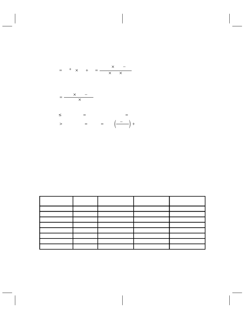
on values of 0, 1, 2, or 3 which correspond to division factors of 1, 2, 4, or 8. The Q-divider register (Q) is
stored in bits 2 – 0 of the MCLK/loop clock control register (index: 0x39) and can take on values of 0, 1, 2,
. . ., 7 which correspond to division factors of 2, 4, 6, . . ., 16. The total post-scalar frequency division factor
is:
F
VCO
4
F
D
Z
2
P
1
(Q
1)
(65
N)
K
(7)
Next, set F
VCO
to the lower limit of 110 MHz and solve for Z:
27.5
(65
F
D
Z
N)
K
(8)
Finally, determine the P and Q values:
IF Z
16 then P
TRUNC (log
2
Z), Q
0
IF Z
16 then P
3, Q
INT
Z
16
16
1
Set bits 7,6 of the N-value register to 1,1 (default). Set LES1 and LES0 in the M-value register (bits 7,6) to
0,0 (default). Set bits 7–2 of the P-value register to 1111 00. This enables the PLL to oscillate and disables
the LCLK edge synchronizer function, which is only used for packed-24 modes. To reset the PLL by resetting
bit 7 of the P-value register to 0.
2.4.3.2
For packed-24 modes, the loop clock PLL is programmed according to Table 2–15. The LCLK edge
synchronizer delay (M-value register bits 7 and 6) depends on whether the graphics accelerator is driving
the VRAM shift clock (true color control register bit TCR5 is cleared to 0) or the TVP3026 is driving the VRAM
shift clock (TCR5 = 1). See subsection 2.6.6, Packed-24 Mode for a typical setup procedure for packed-24
modes. As shown in Table 2–15, a different setting is required for the M-value register in the 4:3 multiplex
mode depending on the silicon revision. Software can determine the silicon revision by reading the silicon
revision register at index 0x01 (a value
≤
0x20 indicates revision A and
≥
0x21 indicates revision B).
Programming for Packed-24 Modes
Table 2–15. Loop Clock PLL Settings for Packed-24 Mode
PACKED-24 MODE
BIT TCR5
(Index 0x18)
N-VALUE REGISTER
M-VALUE REGISTER
TVP3026A
M-VALUE REGISTER
TVP3026B
4:3
0
0xFD
0
×
F9
0
×
FC
0
×
FC
0
×
FD
0
×
F9
0
×
FC
0
×
FC
0
×
BE
0
×
BE
0
×
3D
0
×
7F
0
×
3E
0
×
3E
0
×
BD
0
×
FF
0x3E
0
×
BE
0
×
3D
0
×
7F
0
×
BE
0
×
3E
0
×
BD
0
×
FF
8:3
0
5:4
0
5:2
0
4:3
1
8:3
1
5:4
1
5:2
1
相關(guān)PDF資料 |
PDF描述 |
|---|---|
| TVP3026-175M | Video Interface PALETTE Exract(組合像素模式視頻接口調(diào)色器) |
| TVP3026-220 | Video Interface PALETTE Exract(組合像素模式視頻接口調(diào)色器) |
| TVP3026-250 | Video Interface PALETTE Exract(組合像素模式視頻接口調(diào)色器) |
| TX24 | 60.8 MM 5 X 8 DOT MATRIX DISPLAYS |
| TXB0102DCTR | 2-BIT BIDIRECTIONAL VOLTAGE-LEVEL TRANSLATOR WITH AUTO DIRECTION SENSING AND 【15-kV ESD PROTECTION |
相關(guān)代理商/技術(shù)參數(shù) |
參數(shù)描述 |
|---|---|
| TVP3026-175AMDN | 制造商:TI 制造商全稱:Texas Instruments 功能描述:Video Interface Palette |
| TVP3026-175APCE | 制造商:TI 制造商全稱:Texas Instruments 功能描述:Video Interface Palette |
| TVP3026-175BMDN | 制造商:TI 制造商全稱:Texas Instruments 功能描述:Video Interface Palette |
| TVP3026175BPCE | 制造商:TI 功能描述:*NEW* |
| TVP3026-175BPCE | 制造商:Rochester Electronics LLC 功能描述:- Bulk |
發(fā)布緊急采購,3分鐘左右您將得到回復(fù)。