- 您現(xiàn)在的位置:買賣IC網(wǎng) > PDF目錄382686 > TSA5511 (NXP SEMICONDUCTORS) 1.3 GHz Bidirectional I2C-bus controlled synthesizer PDF資料下載
參數(shù)資料
| 型號(hào): | TSA5511 |
| 廠商: | NXP SEMICONDUCTORS |
| 元件分類: | XO, clock |
| 英文描述: | 1.3 GHz Bidirectional I2C-bus controlled synthesizer |
| 中文描述: | PLL FREQUENCY SYNTHESIZER, 1300 MHz, PDIP18 |
| 封裝: | 0.300 INCH, PLASTIC, SOT-102, DIP-18 |
| 文件頁數(shù): | 8/19頁 |
| 文件大小: | 145K |
| 代理商: | TSA5511 |
October 1992
8
Philips Semiconductors
Product specification
1.3 GHz Bidirectional I
2
C-bus controlled synthesizer
TSA5511
READ mode : R/W = 1 (see Table 2)
Data can be read out of the TSA5511 by setting the R/W bit to 1. After the slave address has been recognized, the
TSA5511 generates an acknowledge pulse and the first data byte (status word) is transferred on the SDA line (MSB first).
Data is valid on the SDA line during a high position of the SCL clock signal.
A second data byte can be read out of the TSA5511 if the processor generates an acknowledge on the SDA line. End of
transmission will occur if no acknowledge from the processor occurs.
The TSA5511 will then release the data line to allow the processor to generate a STOP condition.
When ports P3 to P7 are used as inputs, they must be programmed in their high-impedance state.
The POR flag (power-on reset) is set to 1 when V
CC
goes below 3 V and at power-on. It is reset when an end of data is
detected by the TSA5511 (end of a READ sequence).
Control of the loop is made possible with the in-lock flag FL which indicates (FL = 1) when the loop is phase-locked. The
bits I2, I1 and I0 represent the status of the I/O ports P7, P5 and P4 respectively. A logic 0 indicates a LOW level and a
logic 1 a HIGH level (TTL levels).
A built-in 5-level ADC is available on I/O port P6. This converter can be used to feed AFC information to the controller
from the IF section of the television as illustrated in the typical application circuit (Fig.5). The relationship between bits
A2, A1 and A0 and the input voltage on port P6 is given in Table 3.
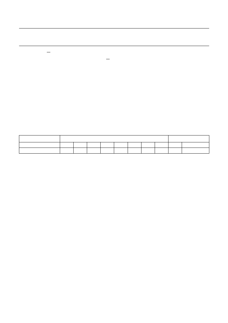
Table 2
Read data format
Note to Table 2
Address selection
The module address contains programmable address bits (MA1 and MA0) which together with the I/O port P3 offers the
possibility of having several synthesizers (up to 3) in one system.
The relationship between MA1 and MA0 and the input voltage I/O port P3 is given in Table 4.
MSB
LSB
Address
Status byte
1
1
0
I2
0
I1
0
I0
MA1
A2
MA0
A1
1
A
byte 1
byte 2
POR
FL
A0
POR
FL
I2, I1, I0
A2, A1, A0
MSB is transmitted first.
power-on reset flag. (POR = 1 on power-on)
in-lock flag (FL = 1 when the loop is phase-locked)
digital information for I/O ports P7, P5 and P4 respectively
digital outputs of the 5-level ADC. Accuracy is 1/2 LSB (see Table 3)
相關(guān)PDF資料 |
PDF描述 |
|---|---|
| TSA5511AT | 1.3 GHz Bidirectional I2C-bus controlled synthesizer |
| TSA5511T | 1.3 GHz Bidirectional I2C-bus controlled synthesizer |
| TSA6057 | Radio tuning PLL frequency synthesizers |
| TSA6057T | Radio tuning PLL frequency synthesizers |
| TSA6060 | Fast radio tuning PLL frequency synthesizer |
相關(guān)代理商/技術(shù)參數(shù) |
參數(shù)描述 |
|---|---|
| TSA5511AT | 制造商:PHILIPS 制造商全稱:NXP Semiconductors 功能描述:1.3 GHz Bidirectional I2C-bus controlled synthesizer |
| TSA5511ATD-T | 制造商:未知廠家 制造商全稱:未知廠家 功能描述:I2C-Bus Frequency Synthesizer |
| TSA5511D | 制造商:未知廠家 制造商全稱:未知廠家 功能描述:I2C-Bus Frequency Synthesizer |
| TSA5511N | 制造商:未知廠家 制造商全稱:未知廠家 功能描述:I2C-Bus Frequency Synthesizer |
| TSA5511T | 制造商:PHILIPS 制造商全稱:NXP Semiconductors 功能描述:1.3 GHz Bidirectional I2C-bus controlled synthesizer |
發(fā)布緊急采購,3分鐘左右您將得到回復(fù)。