- 您現(xiàn)在的位置:買賣IC網(wǎng) > PDF目錄365967 > TS982 RAIL TO RAIL HIGH OUTPUT CURRENT DUAL OPERATIONAL AMPLIFIER PDF資料下載
參數(shù)資料
| 型號: | TS982 |
| 元件分類: | 運(yùn)算放大器 |
| 英文描述: | RAIL TO RAIL HIGH OUTPUT CURRENT DUAL OPERATIONAL AMPLIFIER |
| 中文描述: | 軌對軌高輸出電流雙路運(yùn)算放大器 |
| 文件頁數(shù): | 13/15頁 |
| 文件大?。?/td> | 569K |
| 代理商: | TS982 |
TS982
13/15
APPLICATION INFORMATION
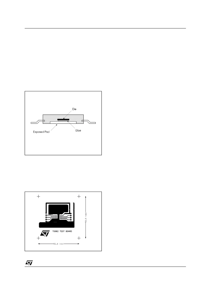
Exposed Pad Package Description
The dual operational amplifier TS982 is housed in
an SO8 Exposed-Pad plastic package. As shown
in the figure below, the die is mounted and glued
on a leadframe. This leadframe is exposed as a
thermal pad on the underside of the package. The
thermal contact is direct with the die and therefore,
offers an excellent thermal performance in com-
parison with usual SO packages. The thermal
contact between the die and the Exposed Pad is
characterized using the parameter R
thjc
.
As 90% of the heat is removed through the pad,
the thermal dissipation of the circuit is directly
linked to the copper area soldered to the pad. In
other words, the R
thja
depends on the copper area
and the number of layers of the printed circuit
board under the pad.
TS982 Testboard layout: 6 cm
2
of copper topside:
Exposed Pad Electrical Connection
In the SO8Epad package, the silicon die is mount-
ed on the thermal pad (see the figure above). The
silicon substrate is not directly connected to the
pad because of the glue. Therefore, the copper
area of the Exposed Pad must be connected to
the substrate voltage (Vcc-) pin4.
Thermal Management Benefits
A good thermal design is important to maintain the
temperature of the silicon junction below
Tj=150°C as given in the Absolute Maximum
Ratings and also to maintain the operating power
level.
Another effect of temperature is that the life ex-
pectancy of an integrated circuit decreases expo-
nentially at extended high temperature operation.
Using one rule-of-thumb, the chip failure rates
double for every 10 to 20°C. This demonstrates
that reducing the junction temperature is also im-
portant to improve the reliability of the amplifier.
Thanks to the high dissipation capability of the
SO8 Epad package, the dual OpAmpTS982 al-
lows lower junction temperature at high current
applications in high ambient temperatures.
Thermal Management Guideline
The following guidelines are a simple procedure to
determine the PCB you should use in order to get
the best from the SO8 Exposed Pad package:
K
The first step is to determine the total pow-
er P
total
to be dissipated by the IC.
P
total
= I
cc
x
V
cc
+ P
amp1
+
x
P
amp2
I
out1
+
V
drop2
x
I
out2
I
cc
x
V
cc
is the DC power needed by the TS982 for
operating with no load. You could refer to the
curve ’Current Consumption vs Supply Voltage’ to
determine Icc versus Vcc and versus temperature.
P
amp1
is the power dissipated by the 1st opera-
tional amplifier to output a signal. If the output sig-
nal can be assimilated to a DC signal, you could
simply calculate the dissipated power using the
Voltage drop curves versus output current, supply
voltage, temperature.
相關(guān)PDF資料 |
PDF描述 |
|---|---|
| TSA1005-40IF | Analog to Digital Converter |
| TSA2000G | TRIAC-FULL-WAVE-OUTPUT OPTOCOUPLER |
| TSA2000J | TRIAC-FULL-WAVE-OUTPUT OPTOCOUPLER |
| TSA5060A | 1.3 GHz I2C-bus controlled low phase noise frequency synthesizer |
| TSA5060AT | 1.3 GHz I2C-bus controlled low phase noise frequency synthesizer |
相關(guān)代理商/技術(shù)參數(shù) |
參數(shù)描述 |
|---|---|
| TS982C3R | 制造商:FUJI 制造商全稱:Fuji Electric 功能描述:Low-Loss Fast Recovery Diode |
| TS982C4R | 制造商:FUJI 制造商全稱:Fuji Electric 功能描述:Low-Loss Fast Recovery Diode |
| TS982C6R | 制造商:FUJI 制造商全稱:Fuji Electric 功能描述:SILICON DIODE |
| TS982C6R_10 | 制造商:FUJI 制造商全稱:Fuji Electric 功能描述:Low-Loss Fast Recovery Diode |
| TS982IDW | 功能描述:運(yùn)算放大器 - 運(yùn)放 Dual Bipolar Oper Amps Wide bandwidth RoHS:否 制造商:STMicroelectronics 通道數(shù)量:4 共模抑制比(最小值):63 dB 輸入補(bǔ)償電壓:1 mV 輸入偏流(最大值):10 pA 工作電源電壓:2.7 V to 5.5 V 安裝風(fēng)格:SMD/SMT 封裝 / 箱體:QFN-16 轉(zhuǎn)換速度:0.89 V/us 關(guān)閉:No 輸出電流:55 mA 最大工作溫度:+ 125 C 封裝:Reel |
發(fā)布緊急采購,3分鐘左右您將得到回復(fù)。