- 您現(xiàn)在的位置:買賣IC網(wǎng) > PDF目錄98287 > TS8387VF 1-CH 8-BIT PROPRIETARY METHOD ADC, PARALLEL ACCESS, CQFP68 PDF資料下載
參數(shù)資料
| 型號: | TS8387VF |
| 元件分類: | ADC |
| 英文描述: | 1-CH 8-BIT PROPRIETARY METHOD ADC, PARALLEL ACCESS, CQFP68 |
| 封裝: | CERAMIC, QFP-68 |
| 文件頁數(shù): | 38/38頁 |
| 文件大小: | 617K |
| 代理商: | TS8387VF |
第1頁第2頁第3頁第4頁第5頁第6頁第7頁第8頁第9頁第10頁第11頁第12頁第13頁第14頁第15頁第16頁第17頁第18頁第19頁第20頁第21頁第22頁第23頁第24頁第25頁第26頁第27頁第28頁第29頁第30頁第31頁第32頁第33頁第34頁第35頁第36頁第37頁當(dāng)前第38頁
TS8387
9/38
Note 10 : Termination load parasitic capacitance derating values :
– 50 ohms or 75 ohms controlled impedance traces properly 50 / 75 ohms terminated : 60 ps / pF or 75 ps per additionnal
ECLinPS load.
– Unterminated ( source terminated ) 75 ohms controlled impedance lines : 100 ps / pF or 150 ps per additionnal ECLinPS
termination load.
Note 11 :apply proper 50 / 75 impedance traces propagation time derating values:
6 ps / mm (155 ps/inch) for TSEV8387 Evaluation Board.
Note 12 : Values for TOD and TDR track each other over temperature, ( 1 percent variation for TOD – TDR per 100 degrees Celsius
temperature variation ). Therefore TOD – TDR variation over temperature is negligible. Moreover, the internal ( onchip ) and
package skews between each Data TODs and TDR effect can be considered as negligible.Consequently, minimum values
for TOD and TDR are never more than 100 ps apart. The same is true for the TOD and TDR maximum values (see Advanced
Application Notes about TOD – TDR variation over temperature in section 7).
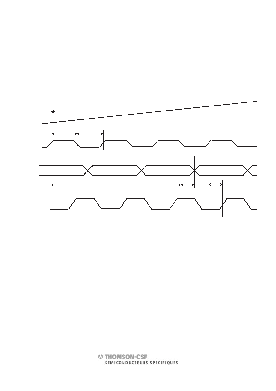
TC1
TC2
DATA N
CLK
TA
X
N+1
X
N+2
X
N+3
PIPELINE DELAY (TPD) : 2.5 CLOCK PERIODS
N
VIN
Figure 1 : TS8387 TIMING DIAGRAM
DATA READY
OUTPUT
DATA N–1
TDR
DIGITAL
OUTPUTS
TOD
DATA N–2
TS8387 principle of operation :
The analog input is sampled on the rising edge of external clock input (CLK,CLKB) after TA (aperture delay) of typically 0
ps .
The digitized data is available after 2.5 clock periods latency (pipeline delay (TPD)), on clock falling edge, after 1100 ps
typical propagation delay TOD.
The Data Ready differential output signal (DR,DRB) switches at external clock frequency, that is at twice the digital
output data rate .
The Data Ready output signal (DR,DRB) switches on external clock falling edge after a propagation delay TDR of typi-
cally 1000 ps.
相關(guān)PDF資料 |
PDF描述 |
|---|---|
| TS8387MF | 1-CH 8-BIT PROPRIETARY METHOD ADC, PARALLEL ACCESS, CQFP68 |
| TS8387VF_ | 1-CH 8-BIT PROPRIETARY METHOD ADC, PARALLEL ACCESS, CQFP68 |
| TS12A4516P | 1-CHANNEL, SGL POLE SGL THROW SWITCH, PDIP8 |
| TS2007EIJT | 3 W, 1 CHANNEL, AUDIO AMPLIFIER, PBGA9 |
| TS2007EKIJT | 3 W, 1 CHANNEL, AUDIO AMPLIFIER, PBGA9 |
相關(guān)代理商/技術(shù)參數(shù) |
參數(shù)描述 |
|---|---|
| TS8388B | 制造商:ATMEL 制造商全稱:ATMEL Corporation 功能描述:ADC 8-bit 1 GSPS |
| TS8388BCF | 制造商:e2v technologies 功能描述:ADC 8-BIT 1 GSPS - Trays |
| TS8388BCFS | 制造商:e2v technologies 功能描述:ADC 8-BIT 1 GSPS - Trays |
| TS8388BCG | 制造商:未知廠家 制造商全稱:未知廠家 功能描述:A/D CONVERTER |
| TS8388BCGL | 制造商:e2v technologies 功能描述:ADC 8-BIT 1 GSPS - Trays |
發(fā)布緊急采購,3分鐘左右您將得到回復(fù)。