- 您現(xiàn)在的位置:買賣IC網(wǎng) > PDF目錄98287 > TS8387MF 1-CH 8-BIT PROPRIETARY METHOD ADC, PARALLEL ACCESS, CQFP68 PDF資料下載
參數(shù)資料
| 型號: | TS8387MF |
| 元件分類: | ADC |
| 英文描述: | 1-CH 8-BIT PROPRIETARY METHOD ADC, PARALLEL ACCESS, CQFP68 |
| 封裝: | CERAMIC, QFP-68 |
| 文件頁數(shù): | 25/38頁 |
| 文件大?。?/td> | 617K |
| 代理商: | TS8387MF |
第1頁第2頁第3頁第4頁第5頁第6頁第7頁第8頁第9頁第10頁第11頁第12頁第13頁第14頁第15頁第16頁第17頁第18頁第19頁第20頁第21頁第22頁第23頁第24頁當前第25頁第26頁第27頁第28頁第29頁第30頁第31頁第32頁第33頁第34頁第35頁第36頁第37頁第38頁
TS8387
31/38
7.7.
OUT OF RANGE BIT
An Out of Range (OR) bit is furnished that goes to logical high state when the input exceeds the positive full scale or falls
below the negative full scale.
When the analog input exceeds the positive full scale, the digital outputs remain at high logical state, with OR at logical
one.
When the analog input falls below the negative full scale, the digital outputs remain at logical low state, with OR at logical
one.
7.8.
GRAY OR BINARY OUTPUT DATA FORMAT SELECT
The TS8387 internal regeneration latches indecision ( for inputs very close to latches threshold) may produce errors in
the logic encoding circuitry and lead to large amplitude output errors.
This is due to the fact that the latches are regenerating the internal analog residues into logical states with a finite volt-
age gain value (Av) within a given positive amount of time
D(t) :
Av= exp(
D(t)/t) , with t the positive feedback regeneration time constant.
The TS8387 has been designed for reducing the probability of occurence of such errors to approximately 10–18 (tar-
getted for the TS8387 at 500 MSPS).
A standard technique for reducing the amplitude of such errors down to +/–1 LSB consists in using Gray code format for
the digital output datas.
Though the TS8387 has been designed for featuring a Bit Error Rate of 10–18 with a binary output format, it is possible for
the user to select between the Binary or Gray output data format , in order to reduce the amplitude of such errors when
occuring, by storing Gray output codes.
Digital Datas format selection :
BINARY output format if GORB is floating or VCC.
GRAY output format if GORB is connected to ground (0V).
7.9.
DIODE PIN 49
The DIODE pin 49 is provided for die junction temperature monitoring.
The operating die junction temperature must be kept below145
°C, therefore an adequate cooling system has to be set
up.
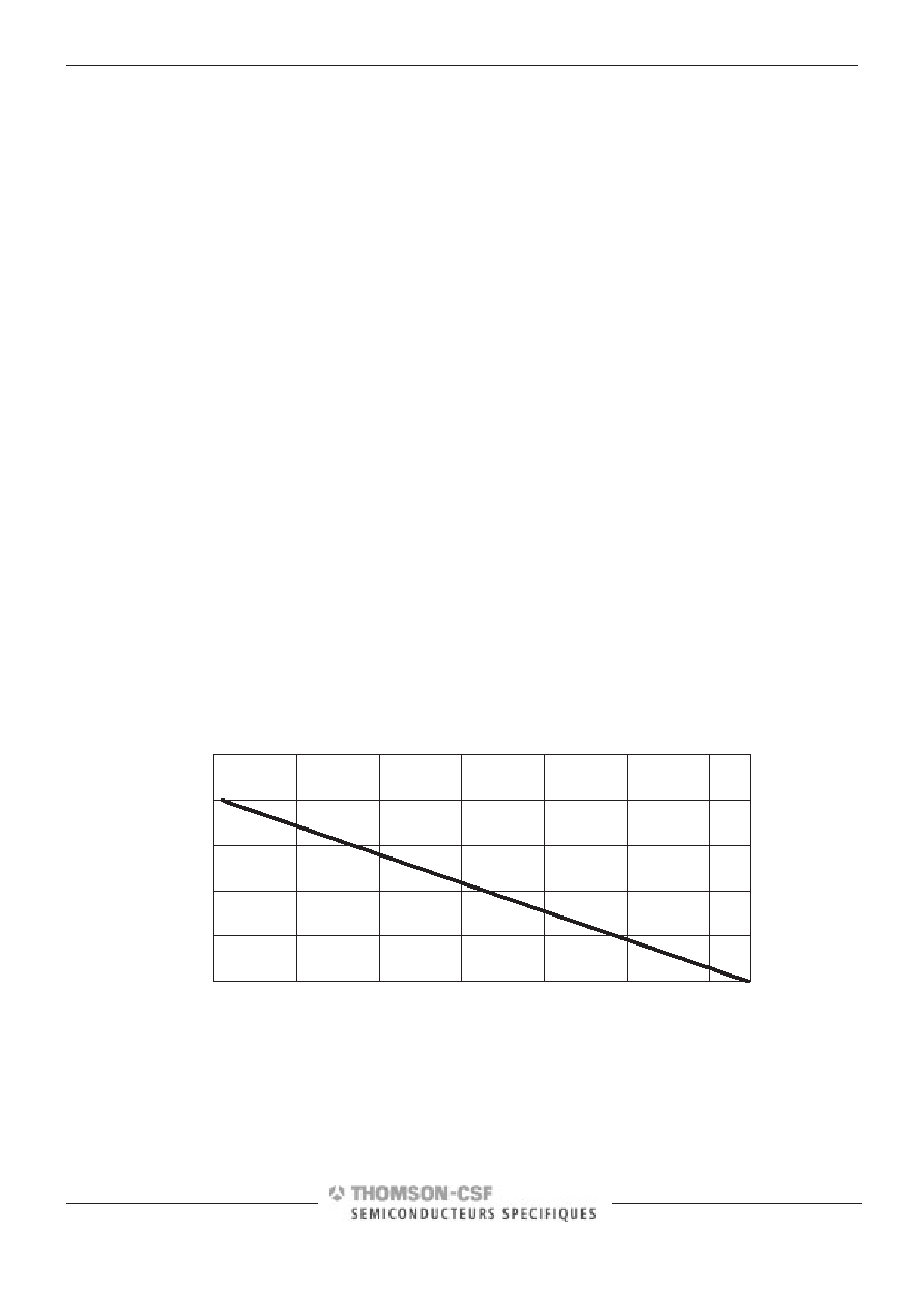
The diode mounted transistor measured Vbe value as a function of junction temperature is given below.
V
oltage
(mV
olts)
Junction temperature (
°C)
550
600
650
700
750
800
20
40
60
80
100
120
140
7.10. OPTIONAL ADC GAIN CONTROL PIN 60 (Non accessible)
The ADC gain is by default not adjustable on the available versions.
However, the possibility exists to adjust the ADC gain by the means of the pin ( 60 ) .
NOTE : This pad is internally shorted to Ground, to avoid any noise immunity related problems on the ADC default ver-
sion.
相關(guān)PDF資料 |
PDF描述 |
|---|---|
| TS8387CF | 1-CH 8-BIT PROPRIETARY METHOD ADC, PARALLEL ACCESS, CQFP68 |
| TS(X)8387CF | 1-CH 8-BIT PROPRIETARY METHOD ADC, PARALLEL ACCESS, CQFP68 |
| TS8387CF_ | 1-CH 8-BIT PROPRIETARY METHOD ADC, PARALLEL ACCESS, CQFP68 |
| TS(X)8387CF_ | 1-CH 8-BIT PROPRIETARY METHOD ADC, PARALLEL ACCESS, CQFP68 |
| TS8387VF | 1-CH 8-BIT PROPRIETARY METHOD ADC, PARALLEL ACCESS, CQFP68 |
相關(guān)代理商/技術(shù)參數(shù) |
參數(shù)描述 |
|---|---|
| TS8388B | 制造商:ATMEL 制造商全稱:ATMEL Corporation 功能描述:ADC 8-bit 1 GSPS |
| TS8388BCF | 制造商:e2v technologies 功能描述:ADC 8-BIT 1 GSPS - Trays |
| TS8388BCFS | 制造商:e2v technologies 功能描述:ADC 8-BIT 1 GSPS - Trays |
| TS8388BCG | 制造商:未知廠家 制造商全稱:未知廠家 功能描述:A/D CONVERTER |
| TS8388BCGL | 制造商:e2v technologies 功能描述:ADC 8-BIT 1 GSPS - Trays |
發(fā)布緊急采購,3分鐘左右您將得到回復(fù)。