- 您現(xiàn)在的位置:買賣IC網(wǎng) > PDF目錄359307 > TS2938ACP55.0 (Taiwan Semiconductor Co., Ltd.) 500mA Ultra Low Dropout Fixed Voltage Regulator with Inhibit PDF資料下載
參數(shù)資料
| 型號(hào): | TS2938ACP55.0 |
| 廠商: | Taiwan Semiconductor Co., Ltd. |
| 英文描述: | 500mA Ultra Low Dropout Fixed Voltage Regulator with Inhibit |
| 中文描述: | 500mA的超低壓差穩(wěn)壓器固定與抑制 |
| 文件頁數(shù): | 2/5頁 |
| 文件大小: | 108K |
| 代理商: | TS2938ACP55.0 |

TS2938/A
2-5
2004/09 rev. A
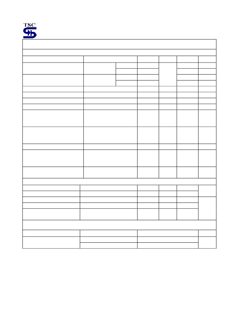
Electrical Characteristics
Vin = Vout + 1V, I
L
= 5mA, C
o
= 6.8uF, Ta = 25
o
C, Vinhibit = 0V, unless otherwise specified.
Parameter
Ta = 25
o
C
Conditions
Min
Typ
Max
Unit
TS2938A
0.990|Vo|
1.010|Vo|
v
Output Voltage
TS2938
0.980|Vo|
1.020|Vo|
V
TS2938A
0.980|Vo|
1.020|Vo|
Output Voltage
Ta = -25 ~ 85
o
C
TS2938
0.960|Vo|
8.0 / 5.0
3.3 / 2.5
1.040|Vo|
V
Input Supply Voltage
--
--
26
V
Output Voltage Temp. Coefficient
Vo+1V
≤
Vin
≤
26V
5mA
≤
I
L
≤
500mA
I
L
=100mA
I
L
=300mA
I
L
=500mA
I
L
=100uA
I
L
=300mA
I
L
=500mA
Vout=0
--
50
150
ppm/
o
C
Line Regulation
--
0.05
0.5
%
Load Regulation
--
0.2
1.0
%
Dropout Voltage (Note 4)
--
--
--
100
300
500
200
400
600
mV
Quiescent Current (Note 5)
--
--
--
100
12
25
200
20
50
uA
mA
Short Circuit Current (Note 6)
--
0.9
1.3
A
Output Noise,
10Hz
to 100KHz, I
L
=10mA
C
L
=2.2uF
C
L
=3.3uF
C
L
=33uF
Io=350mA, f=120Hz,
Co=100uF, Vin=Vo+3V+2Vpp
--
--
--
500
350
120
--
--
--
uVrms
Ripple Rejection Ratio
60
--
--
dB
Shutdown Input
Input Logic Voltage
Low (Regulator ON)
--
1.3
0.7
High (Regulator OFF)
2.0
--
--
V
Shutdown Pin Input Current
Vinhibit = 2.4V
--
30
50
Vinhibit = 26V
Vinhibit
≤
2V, Vin
≤
26V,
Vout = 0V
--
450
600
Regulator Output Current in
Shutdown
Thermal Performance
--
--
200
uA
Condition
Package type
Typ
Unit
TO-252
150
Thermal Resistance
Junction to Ambient
Note 1: Absolute Maximum Rating is limits beyond which damage to the device may occur. For guaranteed Specifications
and test conditions see the Electrical Characteristics.
Note 2: Maximum positive supply voltage of 60V must be limited duration (<100mS) and duty cycle (<1%).
Note 3: The maximum allowable power dissipation is a function of the maximum junction temperature, Tj, the junction to
ambient thermal resistance,
θ
ja, and the ambient temperature, Ta. Exceeding the maximum allowable power
dissipation will cause excessive die temperature, and the regulator will go into thermal shutdown. The effective
value of
θ
ja can be reduced by using a heatsink.
Note 4: Dropout voltage is defined as the input to output differential at which the output voltage drops 2% below its
nominal value measured at 1V differential.
Note 5: Ground pin current is the regulator quiescent current. The total current drawn from the source is the sum of the
ground pin current and output load current.
Note 6: Output current will decrease with increasing temperature, but it will be not dropped below 500mA at the maximum
specified temperature.
SOP-8
170
o
C/W
相關(guān)PDF資料 |
PDF描述 |
|---|---|
| TS2938CS8.0 | 500mA Ultra Low Dropout Fixed Voltage Regulator with Inhibit |
| TS2938ACS8.0 | 500mA Ultra Low Dropout Fixed Voltage Regulator with Inhibit |
| TS39101CS5.0 | 5.0 AMP POSITIVE VOLTAGE REGULATOR |
| TS39101CS3.3 | 5.0 AMP POSITIVE VOLTAGE REGULATOR |
| TS39101CS1.5 | 5.0 AMP POSITIVE VOLTAGE REGULATOR |
相關(guān)代理商/技術(shù)參數(shù) |
參數(shù)描述 |
|---|---|
| TS2938ACP58.0 | 制造商:TSC 制造商全稱:Taiwan Semiconductor Company, Ltd 功能描述:500mA Ultra Low Dropout Fixed Voltage Regulator with Inhibit |
| TS2938ACP580 | 制造商:TSC 制造商全稱:Taiwan Semiconductor Company, Ltd 功能描述:500mA Ultra Low Dropout Fixed Voltage Regulator with Inhibit |
| TS2938ACS | 制造商:TSC 制造商全稱:Taiwan Semiconductor Company, Ltd 功能描述:500mA Ultra Low Dropout Fixed Voltage Regulator with Inhibit |
| TS2938ACS2.5 | 制造商:TSC 制造商全稱:Taiwan Semiconductor Company, Ltd 功能描述:500mA Ultra Low Dropout Fixed Voltage Regulator with Inhibit |
| TS2938ACS25 | 制造商:TSC 制造商全稱:Taiwan Semiconductor Company, Ltd 功能描述:500mA Ultra Low Dropout Fixed Voltage Regulator with Inhibit |
發(fā)布緊急采購,3分鐘左右您將得到回復(fù)。