- 您現(xiàn)在的位置:買賣IC網(wǎng) > PDF目錄68695 > TRU050TDLNA40.96 (VECTRON INTERNATIONAL) PHASE LOCKED LOOP, CDIP16 PDF資料下載
參數(shù)資料
| 型號: | TRU050TDLNA40.96 |
| 廠商: | VECTRON INTERNATIONAL |
| 元件分類: | PLL合成/DDS/VCOs |
| 英文描述: | PHASE LOCKED LOOP, CDIP16 |
| 封裝: | ROHS COMPLIANT, HERMETIC SEALED, CERAMIC, DIP-16 |
| 文件頁數(shù): | 10/14頁 |
| 文件大小: | 0K |
| 代理商: | TRU050TDLNA40.96 |
TRU050, VCXO Based PLL
Vectron International, 267 Lowell Rd, Hudson NH 03051-4916
Tel: 1-88-VECTRON-1
Web: www.vectron.com
Page 5 of 14
Rev : 06Jan2006
VDD
0V
0
+π
π
Relative
Phase (
θ
e)
VDD/2
Vd
Gain Slope = VDD/ 2π
Figure 5. Open Loop Phase Detector Transfer Curve
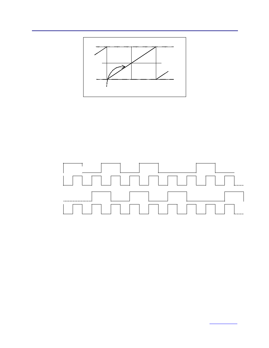
Recovered Clock and Data Alignment Outputs
The TRU050 is designed to recover an imbedded clock from an NRZ data signal and retime it with a data
pattern. In this application, the VCXO frequency is exactly the same frequency as the NRZ data rate and
the outputs are taken off Pin 11, RCLK, and Pin 12, RDATA. Under locked conditions, the falling edge of
RCLK is centered in the RDATA pattern. Also, there is a 1.5 clock cyle delay between DATAIN and
RDATA. Figure 6 shows the relationship between the DATAIN, CLKIN, RDATA and RCLK.
Figure 6. Clock and Data Timing Relationships for the NRZ data
Other RZ encoding schemes such as Manchester or AMI can be accomidated by using a TRU050 at
twice the baud rate.
Loss of Signal, LOS and LOSIN
The LOS circuit provides an output alarm flag when the DATAIN input signal is lost. The LOS output is
normally a logic low and is set to a logic high after 256 consecutive clock periods on CLKIN with no
detected DATAIN transitions. This signal can be used to either flag external alarm circuits and/or drive the
TRU050’s LOSIN input. When LOSIN is set to a logic high, the VCXO control voltage (pin 1) is switched
to an internal voltage which centers OUT1 and OUT2 to center frequency +/-75ppm. Also, LOS
automatically closes the op amp feedback which means the op-amp is a unity gain buffer and will
produce a DC voltage equal to the +op amp voltage (pin 4), usually VDD/2.
Clock In
Data In
Recovered
Data
Recovered Clock
Data1
相關(guān)PDF資料 |
PDF描述 |
|---|---|
| TRU050TECGA12.288 | PHASE LOCKED LOOP, CDIP16 |
| TRU050TECGA40.96 | PHASE LOCKED LOOP, CDIP16 |
| TRU050TECGB25 | PHASE LOCKED LOOP, CDIP16 |
| TRU050TECHA33.33 | PHASE LOCKED LOOP, CDIP16 |
| TRU050TECNA32 | PHASE LOCKED LOOP, CDIP16 |
相關(guān)代理商/技術(shù)參數(shù) |
參數(shù)描述 |
|---|---|
| TRU050-TDLNA-65M0000000 | 制造商:VECTRON 制造商全稱:Vectron International, Inc 功能描述:Complete VCXO based Phase-Locked Loop |
| TRU050-TDLNB-1M0000000 | 制造商:VECTRON 制造商全稱:Vectron International, Inc 功能描述:Complete VCXO based Phase-Locked Loop |
| TRU050-TDLNB-65M0000000 | 制造商:VECTRON 制造商全稱:Vectron International, Inc 功能描述:Complete VCXO based Phase-Locked Loop |
| TRU050-TECCA | 制造商:未知廠家 制造商全稱:未知廠家 功能描述:SINGLE DROP IN QUARTZ STABILIZED PLL SOLUTUION |
| TRU050-TECFA | 制造商:未知廠家 制造商全稱:未知廠家 功能描述:SINGLE DROP IN QUARTZ STABILIZED PLL SOLUTUION |
發(fā)布緊急采購,3分鐘左右您將得到回復(fù)。