- 您現(xiàn)在的位置:買賣IC網(wǎng) > PDF目錄385944 > TP2640N3-G (SUPERTEX INC) P- Channel Enhancement-Mode Vertical DMOS FETs PDF資料下載
參數(shù)資料
| 型號(hào): | TP2640N3-G |
| 廠商: | SUPERTEX INC |
| 元件分類: | 功率晶體管 |
| 英文描述: | P- Channel Enhancement-Mode Vertical DMOS FETs |
| 中文描述: | 180 mA, 400 V, P-CHANNEL, Si, SMALL SIGNAL, MOSFET, TO-92 |
| 封裝: | GREEN PACKAGE-3 |
| 文件頁(yè)數(shù): | 2/5頁(yè) |
| 文件大小: | 572K |
| 代理商: | TP2640N3-G |
2
TP2635/TP2640
Electrical Characteristics
(T
J
= 25°C unless otherwise specified)
Symbol
Parameter
Drain-to-source break-
down voltage
V
GS(th)
ΔV
GS(th)
I
GSS
Min
-400
-350
-0.8
-
-
Typ
Max
Units
Conditions
BV
DSS
TP2640
TP2635
-
-
V
V
GS
= 0V, I
D
= -2.0mA
Gate threshold voltage
Change in V
GS(th)
with temperature
Gate body leakage
-
-
-2.0
5
-100
-1.0
-10.0
V
V
GS
= V
DS
, I
D
= -1.0mA
V
GS
= V
DS
, I
D
= -1.0mA
V
GS
= ±20V, V
DS
= 0V
V
DS
= -100V, V
GS
= 0V
V
DS
= Max rating, V
GS
= 0V
V
DS
= 0.8 Max Rating,
V
GS
= 0V, T
A
= 125
O
C
V
GS
= -10V, V
DS
= -25V
V
GS
= -2.5V, I
D
= -200mA
V
GS
= -4.5V, I
D
= -150mA
V
GS
= -10V, I
D
= -300mA
V
GS
= -10V, I
D
= -300mA
V
DS
= -25V, I
D
= -300mA
mV/
O
C
nA
μA
μA
I
DSS
Zero gate voltage drain current
-
-
-1.0
mA
I
D(ON)
ON-state drain current
0.7
-
-
A
R
DS(ON)
Static drain-to-source ON-state
resistance
-
12
11
11
-
-
-
-
-
-
-
-
-
-
300
15
15
15
0.75
-
300
50
12
10
15
60
40
-1.8
-
Ω
ΔR
DS(ON)
G
FS
C
ISS
C
OSS
C
RSS
t
d(ON)
t
r
t
d(OFF)
t
f
V
SD
t
rr
Notes:
1.All D.C. parameters 100% tested at 25C unless otherwise stated. (Pulse test: 300s pulse, 2% duty cycle.)
2.All A.C. parameters sample tested.
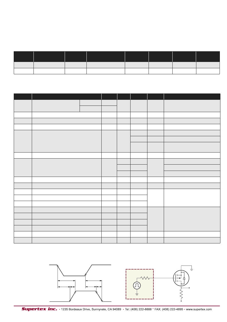
N- Channel Switching Waveforms and Test Circuit
0V
Change in R
DS(ON)
with temperature
Forward transconductance
Input capacitance
Common source output capacitance
Reverse transfer capacitance
Turn-ON delay time
Rise time
Turn-OFF delay time
Fall time
Diode forward voltage drop
Reverse recovery time
-
%/
O
C
m
200
-
-
-
-
-
-
-
-
-
pF
V
GS
= 0V, V
DS
= -25V, f = 1MHz
ns
V
DD
= 25V, I
D
= 2.0A,
R
GEN
= 25
V
ns
V
GS
= 0V, I
SD
= 200mA
V
GS
= 0V, I
SD
= 1.0A
Thermal Characteristics
Package
I
D
(continuous)
1
I
D
(pulsed)
Power Dissipation
@T
C
= 25
O
C
1.3W
2
1.0W
Θ
jc
(
O
C/W)
Θ
jc
(
O
C/W)
I
DR
1
I
DRM
SO-8
TO-92
Notes:
1. I
(continuous) is limited by max rated T
.
2. Mounted on FR4 board, 25mm x 25mm x 1.57mm
-210mA
-180mA
-1.25A
-0.8A
24
125
96
2
170
210mA
-180mA
-1.25A
-0.8A
Ω
90%
10%
90%
90%
10%
10%
PULSE
GENERATOR
V
DD
R
L
OUTPUT
D.U.T.
t
(ON)
t
d(ON)
t
(OFF)
t
d(OFF)
t
F
t
r
INPUT
INPUT
OUTPUT
V
DD
R
gen
0V
-10V
相關(guān)PDF資料 |
PDF描述 |
|---|---|
| TP2635 | P-Channel Enhancement-Mode Vertical DMOS FETs |
| TP2635N3 | P-Channel Enhancement-Mode Vertical DMOS FETs |
| TP2640 | P-Channel Enhancement-Mode Vertical DMOS FETs |
| TP2640LG | P-Channel Enhancement-Mode Vertical DMOS FETs |
| TP2640N3 | P-Channel Enhancement-Mode Vertical DMOS FETs |
相關(guān)代理商/技術(shù)參數(shù) |
參數(shù)描述 |
|---|---|
| TP2640N3-G P002 | 制造商:Supertex Inc 功能描述:P-CH Enhancmnt Mode MOSFET |
| TP2640N3-G P003 | 制造商:Supertex Inc 功能描述:P-CH Enhancmnt Mode MOSFET |
| TP2640N3-G P005 | 制造商:Supertex Inc 功能描述:P-CH Enhancmnt Mode MOSFET |
| TP2640N3-G P013 | 制造商:Supertex Inc 功能描述:P-CH Enhancmnt Mode MOSFET |
| TP2640N3-G P014 | 制造商:Supertex Inc 功能描述:P-CH Enhancmnt Mode MOSFET |
發(fā)布緊急采購(gòu),3分鐘左右您將得到回復(fù)。