- 您現(xiàn)在的位置:買賣IC網(wǎng) > PDF目錄359301 > TMS320C6201B (Texas Instruments, Inc.) DIGITAL SIGNAL PROCESSORS PDF資料下載
參數(shù)資料
| 型號: | TMS320C6201B |
| 廠商: | Texas Instruments, Inc. |
| 元件分類: | 數(shù)字信號處理 |
| 英文描述: | DIGITAL SIGNAL PROCESSORS |
| 中文描述: | 數(shù)字信號處理器 |
| 文件頁數(shù): | 107/123頁 |
| 文件大小: | 1205K |
| 代理商: | TMS320C6201B |
第1頁第2頁第3頁第4頁第5頁第6頁第7頁第8頁第9頁第10頁第11頁第12頁第13頁第14頁第15頁第16頁第17頁第18頁第19頁第20頁第21頁第22頁第23頁第24頁第25頁第26頁第27頁第28頁第29頁第30頁第31頁第32頁第33頁第34頁第35頁第36頁第37頁第38頁第39頁第40頁第41頁第42頁第43頁第44頁第45頁第46頁第47頁第48頁第49頁第50頁第51頁第52頁第53頁第54頁第55頁第56頁第57頁第58頁第59頁第60頁第61頁第62頁第63頁第64頁第65頁第66頁第67頁第68頁第69頁第70頁第71頁第72頁第73頁第74頁第75頁第76頁第77頁第78頁第79頁第80頁第81頁第82頁第83頁第84頁第85頁第86頁第87頁第88頁第89頁第90頁第91頁第92頁第93頁第94頁第95頁第96頁第97頁第98頁第99頁第100頁第101頁第102頁第103頁第104頁第105頁第106頁當前第107頁第108頁第109頁第110頁第111頁第112頁第113頁第114頁第115頁第116頁第117頁第118頁第119頁第120頁第121頁第122頁第123頁
www.ti.com
20
15
SPISIMO
SPISOMI
SPICLK
(clock polarity = 1)
SPICLK
(clock polarity = 0)
SPISIMO Data
Must Be Valid
SPISOMI Data Is Valid
19
16
14
13
12
SPISTE
(A)
TMS320F2808, TMS320F2806
TMS320F2801, UCD9501
Digital Signal Processors
SPRS230F–OCTOBER 2003–REVISED SEPTEMBER 2005
A.
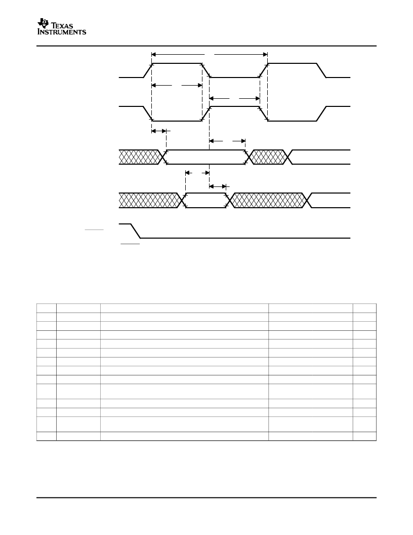
In the slave mode, the SPISTE signal should be asserted low at least 0.5t
c(SPC)
(minimum) before the valid SPI clock
edge and remain low for at least 0.5t
c(SPC)
after the receiving edge (SPICLK) of the last data bit.
Figure 6-19. SPI Slave Mode External Timing (Clock Phase = 0)
Table 6-35. SPI Slave Mode External Timing (Clock Phase = 1)
(1)(2)(3)(4)
NO.
12
13
MIN
MAX
UNIT
ns
ns
ns
ns
ns
ns
ns
ns
ns
t
c(SPC)S
t
w(SPCH)S
t
w(SPCL)S
t
w(SPCL)S
t
w(SPCH)S
t
su(SOMI-SPCH)S
t
su(SOMI-SPCL)S
t
v(SPCH-SOMI)S
t
v(SPCL-SOMI)S
Cycle time, SPICLK
Pulse duration, SPICLK high (clock polarity = 0)
Pulse duration, SPICLK low (clock polarity = 1)
Pulse duration, SPICLK low (clock polarity = 0)
Pulse duration, SPICLK high (clock polarity = 1)
Setup time, SPISOMI before SPICLK high (clock polarity = 0)
Setup time, SPISOMI before SPICLK low (clock polarity = 1
Valid time, SPISOMI data valid after SPICLK low (clock polarity = 0)
Valid time, SPISOMI data valid after SPICLK high (clock polarity =
1)
Setup time, SPISIMO before SPICLK high (clock polarity = 0)
Setup time, SPISIMO before SPICLK low (clock polarity = 1)
Valid time, SPISIMO data valid after SPICLK high (clock polarity =
0)
Valid time, SPISIMO data valid after SPICLK low (clock polarity = 1)
8t
c(LCO)
0.5t
c(SPC)S
- 10
0.5t
c(SPC)S
- 10
0.5t
c(SPC)S
- 10
0.5t
c(SPC)S
- 10
0.125t
c(SPC)S
0.125t
c(SPC)S
0.75t
c(SPC)S
0.75t
c(SPC)S
0.5t
c(SPC)S
0.5t
c(SPC)S
0.5t
c(SPC)S
0.5t
c(SPC)S
14
17
18
21
t
su(SIMO-SPCH)S
t
su(SIMO-SPCL)S
t
v(SPCH-SIMO)S
35
35
ns
ns
ns
22
0.5t
c(SPC)S
t
v(SPCL-SIMO)S
0.5t
c(SPC)S
ns
(1)
(2)
(3)
The MASTER / SLAVE bit (SPICTL.2) is cleared and the CLOCK PHASE bit (SPICTL.3) is cleared.
t
= SPI clock cycle time = LSPCLK/4 or LSPCLK/(SPIBRR + 1)
Internal clock prescalers must be adjusted such that the SPI clock speed is limited to the following SPI clock rate:
Master mode transmit 25-MHz MAX, master mode receive 12.5-MHz MAX
Slave mode transmit 12.5-MHz MAX, slave mode receive 12.5-MHz MAX.
The active edge of the SPICLK signal referenced is controlled by the CLOCK POLARITY bit (SPICCR.6).
(4)
Electrical Specifications
107
相關PDF資料 |
PDF描述 |
|---|---|
| TMS320E25 | SECOND-GENERATION DIGITAL SIGNAL PROCESSORS |
| TMS320LC2402PG | DSP CONTROLLERS |
| TMS320LC2402PGE | DSP CONTROLLERS |
| TMS320UVC5402PGE | FIXED-POINT DIGITAL SIGNAL PROCESSOR |
| TMS320C6202BPYP167 | FIXED-POINT DIGITAL SIGNAL PROCESSORS |
相關代理商/技術參數(shù) |
參數(shù)描述 |
|---|---|
| TMS320C6201BGJC-167 | 制造商:未知廠家 制造商全稱:未知廠家 功能描述:32-Bit Digital Signal Processor |
| TMS320C6201BGJC-200 | 制造商:未知廠家 制造商全稱:未知廠家 功能描述:32-Bit Digital Signal Processor |
| TMS320C6201BGJC-233 | 制造商:未知廠家 制造商全稱:未知廠家 功能描述:32-Bit Digital Signal Processor |
| TMS320C6201BGJL-167 | 制造商:未知廠家 制造商全稱:未知廠家 功能描述:32-Bit Digital Signal Processor |
| TMS320C6201BGJL-200 | 制造商:未知廠家 制造商全稱:未知廠家 功能描述:32-Bit Digital Signal Processor |
發(fā)布緊急采購,3分鐘左右您將得到回復。