- 您現(xiàn)在的位置:買(mǎi)賣(mài)IC網(wǎng) > PDF目錄384010 > TLV320AIC11I (Texas Instruments, Inc.) General-Purpose Low-Voltage 1.1V to 3.6V/0 16-bit 22-KSPS DSP CODEC PDF資料下載
參數(shù)資料
| 型號(hào): | TLV320AIC11I |
| 廠商: | Texas Instruments, Inc. |
| 元件分類(lèi): | Codec |
| 英文描述: | General-Purpose Low-Voltage 1.1V to 3.6V/0 16-bit 22-KSPS DSP CODEC |
| 中文描述: | 通用低電壓1.1V至3.6V的/ 0 16位22 kSPS的DSP的解碼器 |
| 文件頁(yè)數(shù): | 16/55頁(yè) |
| 文件大小: | 263K |
| 代理商: | TLV320AIC11I |
第1頁(yè)第2頁(yè)第3頁(yè)第4頁(yè)第5頁(yè)第6頁(yè)第7頁(yè)第8頁(yè)第9頁(yè)第10頁(yè)第11頁(yè)第12頁(yè)第13頁(yè)第14頁(yè)第15頁(yè)當(dāng)前第16頁(yè)第17頁(yè)第18頁(yè)第19頁(yè)第20頁(yè)第21頁(yè)第22頁(yè)第23頁(yè)第24頁(yè)第25頁(yè)第26頁(yè)第27頁(yè)第28頁(yè)第29頁(yè)第30頁(yè)第31頁(yè)第32頁(yè)第33頁(yè)第34頁(yè)第35頁(yè)第36頁(yè)第37頁(yè)第38頁(yè)第39頁(yè)第40頁(yè)第41頁(yè)第42頁(yè)第43頁(yè)第44頁(yè)第45頁(yè)第46頁(yè)第47頁(yè)第48頁(yè)第49頁(yè)第50頁(yè)第51頁(yè)第52頁(yè)第53頁(yè)第54頁(yè)第55頁(yè)
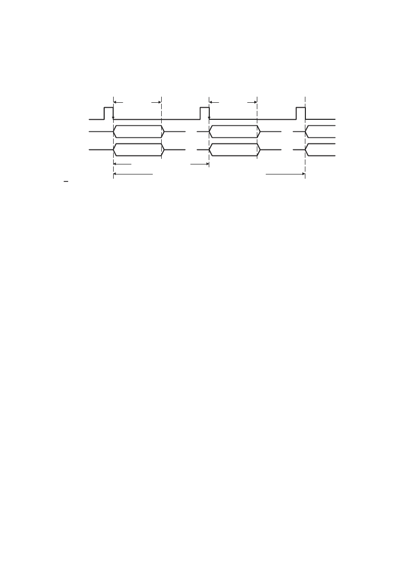
2–2
FS
DOUT
(16-bit)
DOUT
(15+1-bit)
Primary
Secondary
16 SCLKs
# SCLKs Per Sampling Period (See Note C)
16–bit ADC Data
15–bit ADC Data + M/S
M/S+ Register Data/
M/S+ All 0 (See Note A)
# SCLKs (See Note B)
M/S+ Register Data/
M/S+ All 0 (See Note A)
Primary
16 SCLKs
NOTES: A. M/S bit (D15) in the secondary communication is used to indicate whether the register data (address and content) come from a
master device or a slave device if read bit is set. Otherwise, it is all 0s except M/S bit (master: M/S=1, slave: M/S=0).
B. The number of SCLKs between FS (primary) and FS (secondary) is 128 if cascading devices are less than 5, or 256 if cascading
devices are greater than 4.
C. The number of SCLKs per data sampling period is 256 if cascading devices are less than 5, or 512 if cascading devices are greater
than 4.
Figure 2–2. Timing Sequence of ADC Channel (Primary and Secondary Communication)
2.1.3
DAC Signal Channel
DIN received the 16-bit serial data word (2s complement) from the host during the primary communication interval.
These 16-bit digital words, representing analog output signal before PGA, are clocked into the serial port (DIN) at
the falling edge of SCLK during the frame-sync interval, one bit for each SCLK and one word for each primary
communication interval. The data are converted to a pulse train by the sigma-delta DAC comprised of a
digital-interpolation filter and a digital 1-bit modulator. The output of the modulator is then passed to an internal
low-pass filter to complete the signal reconstruction. Finally, the resulting analog signal is applied to the input of a
programmable-gain amplifier is capable of differentially driving a 600-ohm load at OUTP and OUTM. The timing
sequence is shown in Figure 2–3.
During secondary communication, the digital control and configuration data, together with the register address, are
clocked in through DIN (see Appendix A for register map). These 16-bit data are used either to initialize the register
or read out register content through DOUT. If a register initialization is not required, a no-operation word (D15-D9 are
all set to 0) can be used. If D12 is set to 1, the content of the control register, specified by D7-D0, will be send out
through DOUT during the same secondary communication (see section 2.1.5). The timing sequence is shown in
Figure 2–4.
The interpolation FIR filter can be bypassed by writing a 1to bit D1 of control register 1. The whole DAC channel can
be turned off for power savings by writing 10to bits D2 and D1 of control register 3.
相關(guān)PDF資料 |
PDF描述 |
|---|---|
| TLV320AIC34_1 | FOUR-CHANNEL, LOW-POWER AUDIO CODEC FOR PORTABLE AUDIO/TELEPHONY |
| TLV3701CDBV | FAMILY OF NANOPOWER PUSH-PULL OUTPUT COMPARATORS |
| TLV3701IDBV | FAMILY OF NANOPOWER PUSH-PULL OUTPUT COMPARATORS |
| TLV5510INS | 2.7-V TO 3.6-V 8-BIT HIGH-SPEED ANALOG-TO-DIGITAL CONVERTER |
| TLV5535PW | 8-BIT, 35 MSPS, LOW-POWER ANALOG-TO-DIGITAL CONVERTER |
相關(guān)代理商/技術(shù)參數(shù) |
參數(shù)描述 |
|---|---|
| TLV320AIC11IPFB | 功能描述:接口—CODEC Gen Purp Lo-I/O Vltg 16-Bit 22-KSPS DSP RoHS:否 制造商:Texas Instruments 類(lèi)型: 分辨率: 轉(zhuǎn)換速率:48 kSPs 接口類(lèi)型:I2C ADC 數(shù)量:2 DAC 數(shù)量:4 工作電源電壓:1.8 V, 2.1 V, 2.3 V to 5.5 V 最大工作溫度:+ 85 C 安裝風(fēng)格:SMD/SMT 封裝 / 箱體:DSBGA-81 封裝:Reel |
| TLV320AIC11IPFBG4 | 功能描述:接口—CODEC 12-Bit To 24-Bit Reg Bus Exchg W/3-St Otp RoHS:否 制造商:Texas Instruments 類(lèi)型: 分辨率: 轉(zhuǎn)換速率:48 kSPs 接口類(lèi)型:I2C ADC 數(shù)量:2 DAC 數(shù)量:4 工作電源電壓:1.8 V, 2.1 V, 2.3 V to 5.5 V 最大工作溫度:+ 85 C 安裝風(fēng)格:SMD/SMT 封裝 / 箱體:DSBGA-81 封裝:Reel |
| TLV320AIC11PFB | 制造商:TI 制造商全稱(chēng):Texas Instruments 功能描述:General-Purpose Low-Voltage 1.1V to 3.6V/0 16-bit 22-KSPS DSP CODEC |
| TLV320AIC12 | 制造商:TI 制造商全稱(chēng):Texas Instruments 功能描述:PRODUCT NOTIFICATION |
| TLV320AIC12_07 | 制造商:TI 制造商全稱(chēng):Texas Instruments 功能描述:LOW-POWER, HIGHLY-INTEGRATED, PROGRAMMABLE 16-Bit, 26-KSPS MONO CODEC |
發(fā)布緊急采購(gòu),3分鐘左右您將得到回復(fù)。