- 您現(xiàn)在的位置:買賣IC網(wǎng) > PDF目錄384004 > TLC320AD80C (Texas Instruments, Inc.) Audio Processor Subsystem PDF資料下載
參數(shù)資料
| 型號: | TLC320AD80C |
| 廠商: | Texas Instruments, Inc. |
| 英文描述: | Audio Processor Subsystem |
| 中文描述: | 音頻處理器子系統(tǒng) |
| 文件頁數(shù): | 10/36頁 |
| 文件大小: | 219K |
| 代理商: | TLC320AD80C |
第1頁第2頁第3頁第4頁第5頁第6頁第7頁第8頁第9頁當(dāng)前第10頁第11頁第12頁第13頁第14頁第15頁第16頁第17頁第18頁第19頁第20頁第21頁第22頁第23頁第24頁第25頁第26頁第27頁第28頁第29頁第30頁第31頁第32頁第33頁第34頁第35頁第36頁
1–5
1.6
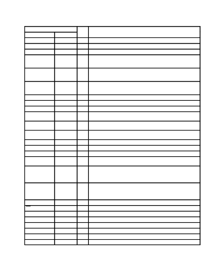
Terminal Functions
TERMINAL
NAME
AGND1
I/O
DESCRIPTION
NO.
18
I
Analog ground for sigma-delta DAC
AGND2
45
I
Analog ground for analog audio output drivers
AGND3
52
I
Analog ground for bandgap reference
AUDIO LEFT
35
O
Left channel line-level analog audio output. The AUDIO LEFT output driver
provides line level signals (1 Vrms max) for line output. The AUDIO LEFT
output is capable of driving a 600-
load.
AUDIO MONO
39
O
Monaural variable line-level analog audio output. The AUDIO MONO output
signal is the sum of the AUDIO RIGHT and AUDIO LEFT outputs divided by
2. The output is capable of driving a 10-k
load.
AUDIO RIGHT
38
O
Right channel variable line-level analog audio output. The AUDIO RIGHT
output driver provides line level signals (1 Vrms max) for line output. The
AUDIO RIGHT output is capable of driving a 600-
load.
AUX AUDIO1L
21
I
Left channel auxiliary analog audio input 1
AUX AUDIO1R
23
I
Right channel auxiliary analog audio input 1
AUX AUDIO2M
24
I
Mono channel auxiliary analog audio input 2
ABCLK
12
I/O
Auxiliary serial bit clock input. The ABCLK bit clock signal clocks the serial
PCM data (ASDATA) into the TLC320AD80.
Auxiliary left/right channel indicator. ALRCLK signifies whether the serial
PCM data is associated with the left channel DAC or the right channel DAC.
Auxiliary serial PCM data input port. ASDATA can be configured as 16 or 18
bits with the most significant bit (MSB) first, 2’s complement format.
Analog 5-V power supply for the sigma-delta DAC
ALRCLK
13
I/O
ASDATA
11
I
AVDD1
AVDD2
AVDD3
BCLK
14
I
44
I
Analog 5-V power supply for the analog audio output drivers
50
I
Analog 5-V power supply for the bandgap reference
9
I
Serial bit clock input. BCLK clocks the serial PCM data (SDATA) into the
device.
Bandgap reference filter. BGFLTR provides for noise filtering of the internal
bandgap reference (2.25 V). BGFLTR requires a 0.1
μ
F capacitor to analog
ground. This voltage node should be loaded only with a high-impedance dc
load.
BGFLTR
46
I
CDIN
61
I
SPI bus serial control data input. Data is transferred MSB first. CDIN
specifies the channel specific attenuation and mute, serial PCM data format
and rates, de-emphasis mode, audio input port selection, and stereo or
monaural analog inputs.
CDOUT
62
O
SPI bus serial control data output port
CS
59
I
SPI bus chip select input (active low)
DGND1
6
I
Digital ground for the sigma-delta DAC
DGND2
58
I
Digital ground for the serial interface
DVDD1
DVDD2
EXT INL
5
I
Digital 5-V power supply for the sigma-delta DAC
57
I
Digital 5-V power supply for the serial interface
26
I
Left channel external analog audio input
EXT INR
27
I
Right channel external analog audio input
相關(guān)PDF資料 |
PDF描述 |
|---|---|
| TLC320AD81CDBT | Stereo Audio Digital Equalizer DC |
| TLC320AD81C | Stereo Audio Digital Equalizer DC |
| TLC339CDB | LinCMOSE MICROPOWER QUAD COMPARATORS |
| TLC339CDBR | LinCMOSE MICROPOWER QUAD COMPARATORS |
| TLC34058-110M | 256 ?24 COLOR PALETTE |
相關(guān)代理商/技術(shù)參數(shù) |
參數(shù)描述 |
|---|---|
| TLC320AD80CPM | 制造商:Rochester Electronics LLC 功能描述:- Bulk 制造商:Texas Instruments 功能描述: |
| TLC320AD81C | 制造商:TI 制造商全稱:Texas Instruments 功能描述:Stereo Audio Digital Equalizer DC |
| TLC320AD81CDBT | 制造商:Rochester Electronics LLC 功能描述:- Tape and Reel |
| TLC320AD90 | 制造商:TI 制造商全稱:Texas Instruments 功能描述:Stereo Audio Codec |
| TLC320AD91 | 制造商:TI 制造商全稱:Texas Instruments 功能描述:Stereo Audio Codec |
發(fā)布緊急采購,3分鐘左右您將得到回復(fù)。