- 您現(xiàn)在的位置:買賣IC網(wǎng) > PDF目錄385929 > TLC2654AQ8D (Texas Instruments, Inc.) Advanced LinCMOSE LOW-NOISE CHOPPER-STABILIZED OPERATIONAL AMPLIFIERS PDF資料下載
參數(shù)資料
| 型號(hào): | TLC2654AQ8D |
| 廠商: | Texas Instruments, Inc. |
| 英文描述: | Advanced LinCMOSE LOW-NOISE CHOPPER-STABILIZED OPERATIONAL AMPLIFIERS |
| 中文描述: | 高級(jí)LinCMOSE低噪聲斬波穩(wěn)定運(yùn)算放大器 |
| 文件頁數(shù): | 20/30頁 |
| 文件大小: | 443K |
| 代理商: | TLC2654AQ8D |
第1頁第2頁第3頁第4頁第5頁第6頁第7頁第8頁第9頁第10頁第11頁第12頁第13頁第14頁第15頁第16頁第17頁第18頁第19頁當(dāng)前第20頁第21頁第22頁第23頁第24頁第25頁第26頁第27頁第28頁第29頁第30頁
0
– 50
0
10
20
t – Time – ms
30
40
V
– 5
0
50
60
70
80
V
VDD
±
=
±
5 V
TA = 25
°
C
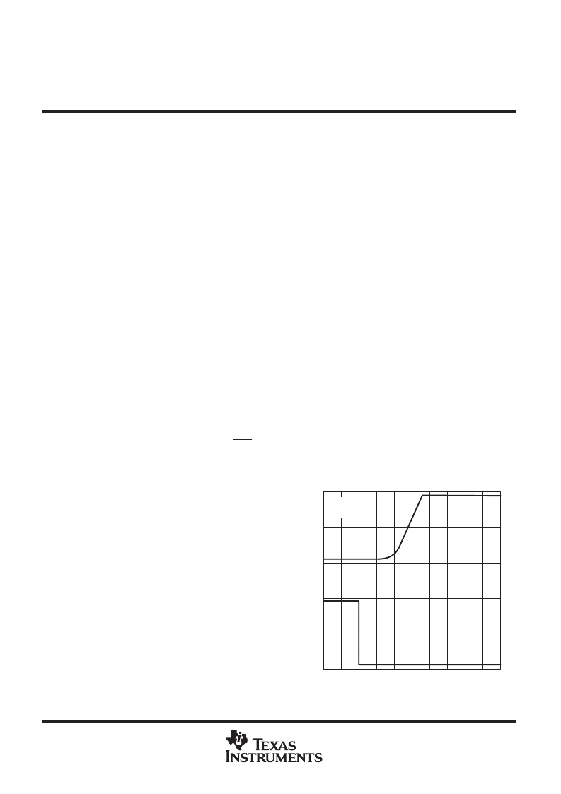
Figure 34. Overload Recovery
TLC2654, TLC2654A
Advanced LinCMOS
LOW-NOISE CHOPPER-STABILIZED
OPERATIONAL AMPLIFIERS
SLOS020F – NOVEMBER 1988 – REVISED JULY 1999
20
POST OFFICE BOX 655303
DALLAS, TEXAS 75265
APPLICATION INFORMATION
capacitor selection and placement
Leakage and dielectric absorption are the two important factors to consider when selecting external capacitors
C
XA
and C
XB
. Both factors can cause system degradation, negating the performance advantages realized by
using the TLC2654.
Degradation from capacitor leakage becomes more apparent with increasing temperatures. Low-leakage
capacitors and standoffs are recommended for operation at T
A
= 125
°
C. In addition, guard bands are
recommended around the capacitor connections on both sides of the printed-circuit board to alleviate problems
caused by surface leakage on circuit boards.
Capacitors with high dielectric absorption tend to take several seconds to settle upon application of power, which
directly affects input offset voltage. In applications needing fast settling of input voltage, high-quality film
capacitors such as mylar, polystyrene, or polypropylene should be used. In other applications, a ceramic or
other low-grade capacitor can suffice.
Unlike many choppers available today, the TLC2654 is designed to function with values of C
XA
and C
XB
in the
range of 0.1
μ
F to 1
μ
F without degradation to input offset voltage or input noise voltage. These capacitors
should be located as close as possible to C
XA
and C
XB
and return to either V
DD–
or C RETURN. On many
choppers, connecting these capacitors to V
DD–
causes degradation in noise performance; this problem is
eliminated on the TLC2654.
internal/external clock
The TLC2654 has an internal clock that sets the chopping frequency to a nominal value of 10 kHz. On 8-pin
packages, the chopping frequency can only be controlled by the internal clock; however, on all 14-pin packages
and the 20-pin FK package the device chopping frequency can be set by the internal clock or controlled
externally by use of the INT/EXT and CLK IN. To use the internal 10-kHz clock, no connection is necessary. If
external clocking is desired, connect INT/EXT to V
DD–
and the external clock to CLK IN. The external clock trip
point is 2.5 V above the negative rail; however, CLK IN can be driven from the negative rail to 5 V above the
negative rail. This allows the TLC2654 to be driven directly by 5-V TTL and CMOS logic when operating in the
single-supply configuration. If this 5-V level is exceeded, damage could occur to the device unless the current
into CLK IN is limited to
±
5 mA. A divide-by-two
frequency divider interfaces with CLK IN and sets
the chopping frequency. The chopping frequency
appears on CLK OUT.
overload recovery/output clamp
When large differential-input-voltage conditions
are applied to the TLC2654, the nulling loop
attempts to prevent the output from saturating by
driving C
XA
and C
XB
to internally-clamped voltage
levels. Once the overdrive condition is removed,
a period of time is required to allow the built-up
charge to dissipate. This time period is defined as
overload recovery time (see Figure 34). Typical
overload recovery time for the TLC2654 is
significantly faster than competitive products;
however, this time can be reduced further by use
of internal clamp circuitry accessible through
CLAMP if required.
相關(guān)PDF資料 |
PDF描述 |
|---|---|
| TLC271(中文) | LinCMOS Progammable Low-Power Operational Amplifiers(低噪聲運(yùn)放) |
| TLC274(中文) | LinCMOS Precision Quad Operational Amplifier(四路單電源運(yùn)放) |
| TLC279(中文) | LinCMOS Precision Quad Operational Amplifier(四路單電源運(yùn)放) |
| TLC277(中文) | LinCMOS Precision Dual Operational Amplifier(雙組精密單電源運(yùn)放) |
| TLC272(中文) | LinCMOS Precision Dual Operational Amplifier(雙路單電源運(yùn)放) |
相關(guān)代理商/技術(shù)參數(shù) |
參數(shù)描述 |
|---|---|
| TLC2654AQ-8D | 功能描述:運(yùn)算放大器 - 運(yùn)放 Adv Ln Chopper RoHS:否 制造商:STMicroelectronics 通道數(shù)量:4 共模抑制比(最小值):63 dB 輸入補(bǔ)償電壓:1 mV 輸入偏流(最大值):10 pA 工作電源電壓:2.7 V to 5.5 V 安裝風(fēng)格:SMD/SMT 封裝 / 箱體:QFN-16 轉(zhuǎn)換速度:0.89 V/us 關(guān)閉:No 輸出電流:55 mA 最大工作溫度:+ 125 C 封裝:Reel |
| TLC2654AQ-8DG4 | 功能描述:運(yùn)算放大器 - 運(yùn)放 LinCMOS LoNose Chopr Stabilized OP AMP RoHS:否 制造商:STMicroelectronics 通道數(shù)量:4 共模抑制比(最小值):63 dB 輸入補(bǔ)償電壓:1 mV 輸入偏流(最大值):10 pA 工作電源電壓:2.7 V to 5.5 V 安裝風(fēng)格:SMD/SMT 封裝 / 箱體:QFN-16 轉(zhuǎn)換速度:0.89 V/us 關(guān)閉:No 輸出電流:55 mA 最大工作溫度:+ 125 C 封裝:Reel |
| TLC2654C14DR | 制造商:Texas Instruments 功能描述: |
| TLC2654C-14DR | 功能描述:運(yùn)算放大器 - 運(yùn)放 Low-Noise Chopper-Stabilized RoHS:否 制造商:STMicroelectronics 通道數(shù)量:4 共模抑制比(最小值):63 dB 輸入補(bǔ)償電壓:1 mV 輸入偏流(最大值):10 pA 工作電源電壓:2.7 V to 5.5 V 安裝風(fēng)格:SMD/SMT 封裝 / 箱體:QFN-16 轉(zhuǎn)換速度:0.89 V/us 關(guān)閉:No 輸出電流:55 mA 最大工作溫度:+ 125 C 封裝:Reel |
| TLC2654C-14DRG4 | 功能描述:運(yùn)算放大器 - 運(yùn)放 Low-Noise Chopper-Stabilized RoHS:否 制造商:STMicroelectronics 通道數(shù)量:4 共模抑制比(最小值):63 dB 輸入補(bǔ)償電壓:1 mV 輸入偏流(最大值):10 pA 工作電源電壓:2.7 V to 5.5 V 安裝風(fēng)格:SMD/SMT 封裝 / 箱體:QFN-16 轉(zhuǎn)換速度:0.89 V/us 關(guān)閉:No 輸出電流:55 mA 最大工作溫度:+ 125 C 封裝:Reel |
發(fā)布緊急采購,3分鐘左右您將得到回復(fù)。