- 您現(xiàn)在的位置:買賣IC網(wǎng) > PDF目錄383948 > TISP61511DR-S (BOURNS INC) DUAL FORWARD-CONDUCTING P-GATE THYRISTORS PROGRAMMABLE OVERVOLTAGE PROTECTORS PDF資料下載
參數(shù)資料
| 型號(hào): | TISP61511DR-S |
| 廠商: | BOURNS INC |
| 元件分類: | 保護(hù)電路 |
| 英文描述: | DUAL FORWARD-CONDUCTING P-GATE THYRISTORS PROGRAMMABLE OVERVOLTAGE PROTECTORS |
| 中文描述: | TELECOM, SURGE PROTECTION CIRCUIT, PDSO8 |
| 封裝: | ROHS COMPLIANT, SOP-8 |
| 文件頁數(shù): | 1/9頁 |
| 文件大小: | 360K |
| 代理商: | TISP61511DR-S |
JULY 1995 — REVISED MARCH 2006
Specifications are subject to change without notice.
Customers should verify actual device performance in their specific applications.
TISP61511D Gated Protectors
TISP61511D
DUAL FORWARD-CONDUCTING P-GATE THYRISTORS
PROGRAMMABLE OVERVOLTAGE PROTECTORS
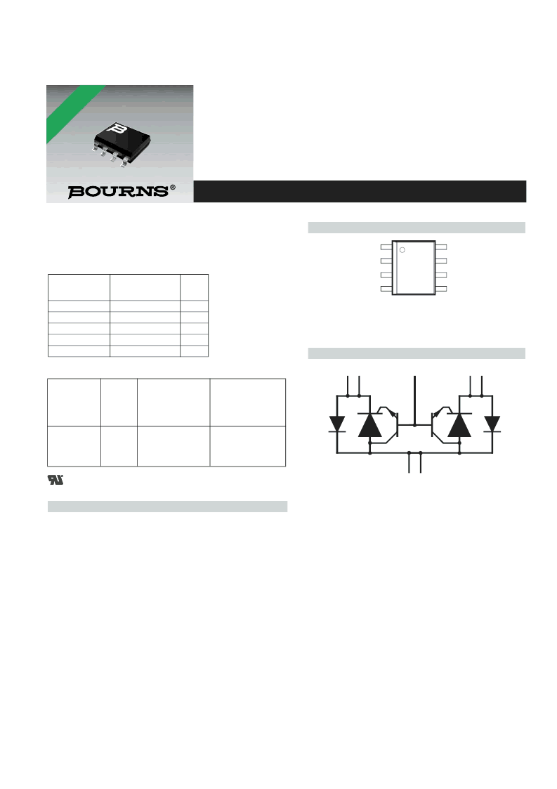
Device Symbol
Dual Voltage-Programmable Protectors.
– Wide 0 to -80 V Programming Range
– Low 5 mA max. Triggering Current
– High 150 mA min. Holding Current
Rated for International Surge Wave Shapes
D Package (Top View)
Description
The TISP61511D is a dual forward-conducting buffered p-gate over-
voltage protector. It is designed to protect monolithic Subscriber Line
Interface Circuits, SLICs, against overvoltages on the telephone line
caused by lightning, ac power contact and induction. The TISP61511D
limits voltages that exceed the SLIC supply rail voltage.
The SLIC line driver section is typically powered from 0 V (ground)
and a negative voltage in the region of -10 V to -70 V. The protector
gate is connected to this negative supply. This references the
protection (clipping) voltage to the negative supply voltage. As the
protection voltage will track the negative supply voltage the overvoltage
stress on the SLIC is minimized.
Voltage Wave
Shape
Standard
I
TSP
A
2/10
μ
s
1.2/50
μ
s
0.5/700
μ
s
10/700
μ
s
10/1000
μ
s
TR-NWT-001089
ETS 300 047-1
RLM88/I3124
K17, K20, K21
TR-NWT-001089
170
90
40
40
30
Functional Replacements for
.............................................. UL Recognized Component
MD6XANB
NC - No internal connection
Terminal typical application names shown in
parenthesis
1
2
3
4
5
6
7
8
K1
A
A
K2
G
K1
K2
NC
(Tip)
(Ground)
(Ground)
(Ring)
(Gate)
(Tip)
(Ring)
Terminals K1, K2 and A correspond to the alternative
line designators of T, R and G or A, B and C. The
negative protection voltage is controlled by the
voltage, V
GG,
applied to the G terminal.
SD6XAE
A
K1
G
K2
Positive overvoltages are clipped to ground by diode forward conduction. Negative overvoltages are initially clipped close to the SLIC negative
supply rail value. If sufficient current is available from the overvoltage, then the protector will crowbar into a low voltage on-state condition. As
the current subsides the high holding current of the crowbar prevents d.c. latchup.
These monolithic protection devices are fabricated in ion-implanted planar vertical power structures for high reliability and in normal system
operation they are virtually transparent. The buffered gate design reduces the loading on the SLIC supply during overvoltages caused by
power cross and induction.
*RoHS Directive 2002/95/EC Jan 27 2003 including Annex
De v c e T p e
Package
Type
LCP1511,
LCP1511D
A T T L7591AS
M G SS 150- 1
8-pin
Small-
Outline
TISP61511D
or TISP61511DR
for Taped and
Reeled
TISP61511D-S
or TISP61511DR-S
for Taped and
Reeled
Functional
Replacement
With Standard
Termination Finish
Order As
Functional
Replacement
With Lead Free
Termination Finish
Order As
*RHAVALABE
VRSONS
發(fā)布緊急采購,3分鐘左右您將得到回復(fù)。