- 您現(xiàn)在的位置:買賣IC網(wǎng) > PDF目錄361449 > TIC236N (Power Innovations International, Inc.) SILICON TRIACS PDF資料下載
參數(shù)資料
| 型號: | TIC236N |
| 廠商: | Power Innovations International, Inc. |
| 英文描述: | SILICON TRIACS |
| 中文描述: | 硅雙向可控硅 |
| 文件頁數(shù): | 1/5頁 |
| 文件大小: | 105K |
| 代理商: | TIC236N |
TIC236 SERIES
SILICON TRIACS
P R O D U C T I N F O R M A T I O N
Information is current as of publication date. Products conform to specifications in accordance
with the terms of Power Innovations standard warranty. Production processing does not
necessarily include testing of all parameters.
1
DECEMBER 1971 - REVISED JUNE 2000
Copyright 2000, Power Innovations Limited, UK
G
High Current Triacs
G
12 A RMS
G
Glass Passivated Wafer
G
400 V to 800 V Off-State Voltage
G
Max I
GT
of 50 mA (Quadrants 1 - 3)
MT1
MT2
G
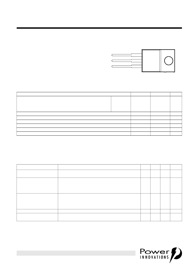
TO-220 PACKAGE
(TOP VIEW)
Pin 2 is in electrical contact with the mounting base.
MDC2ACA
1
2
3
absolute maximum ratings over operating case temperature (unless otherwise noted)
RATING
NOTES: 1. These values apply bidirectionally for any value of resistance between the gate and Main Terminal 1.
2. This value applies for 50-Hz full-sine-wave operation with resistive load. Above 70°C derate linearly to 110°C case temperature at
the rate of 300 mA/°C.
3. This value applies for one 50-Hz full-sine-wave when the device is operating at (or below) the rated value of peak reverse voltage
and on-state current. Surge may be repeated after the device has returned to original thermal equilibrium.
SYMBOL
VALUE
400
600
700
800
12
100
±1
-40 to +110
-40 to +125
230
UNIT
Repetitive peak off-state voltage (see Note 1)
TIC236D
TIC236M
TIC236S
TIC236N
V
DRM
V
Full-cycle RMS on-state current at (or below) 70°C case temperature (see Note 2)
Peak on-state surge current full-sine-wave at (or below) 25°C case temperature (see Note 3)
Peak gate current
Operating case temperature range
Storage temperature range
Lead temperature 1.6 mm from case for 10 seconds
I
T(RMS)
I
TSM
I
GM
T
C
T
stg
T
L
A
A
A
°C
°C
°C
electrical characteristics at 25°C case temperature (unless otherwise noted)
PARAMETER
TEST CONDITIONS
MIN
TYP
MAX
UNIT
I
DRM
Repetitive peak
off-state current
V
D
= Rated V
DRM
I
G
= 0
T
C
= 110°C
±2
mA
I
GT
Gate trigger
current
V
supply
= +12 V
V
supply
= +12 V
V
supply
= -12 V
V
supply
= -12 V
V
supply
= +12 V
V
supply
= +12 V
V
supply
= -12 V
V
supply
= -12 V
I
TM
= ±17 A
V
supply
= +12 V
V
supply
= -12 V
R
L
= 10
R
L
= 10
R
L
= 10
R
L
= 10
R
L
= 10
R
L
= 10
R
L
= 10
R
L
= 10
I
G
= 50 mA
I
G
= 0
I
G
= 0
t
p(g)
> 20
μ
s
t
p(g)
> 20
μ
s
t
p(g)
> 20
μ
s
t
p(g)
> 20
μ
s
t
p(g)
> 20
μ
s
t
p(g)
> 20
μ
s
t
p(g)
> 20
μ
s
t
p(g)
> 20
μ
s
(see Note 4)
Init’ I
TM
= 100 mA
Init’ I
TM
= -100 mA
12
-19
-16
34
0.8
-0.8
-0.8
0.9
±1.4
22
-12
50
-50
-50
mA
V
GT
Gate trigger
voltage
2
-2
-2
2
V
V
T
On-state voltage
±2.1
40
-40
V
I
H
Holding current
mA
All voltages are with respect to Main Terminal 1.
NOTE
4: This parameter must be measured using pulse techniques, t
p
=
≤
1 ms, duty cycle
≤
2 %. Voltage-sensing contacts separate from
the current carrying contacts are located within 3.2 mm from the device body.
相關(guān)PDF資料 |
PDF描述 |
|---|---|
| TIC236S | SILICON TRIACS |
| TIC246 | SILICON TRIACS |
| TIC246D | SILICON TRIACS |
| TIC246M | SILICON TRIACS |
| TIC246N | SILICON TRIACS |
相關(guān)代理商/技術(shù)參數(shù) |
參數(shù)描述 |
|---|---|
| TIC236N-S | 功能描述:雙向可控硅 800V 12A TRIAC RoHS:否 制造商:STMicroelectronics 開啟狀態(tài) RMS 電流 (It RMS):16 A 不重復(fù)通態(tài)電流:120 A 額定重復(fù)關(guān)閉狀態(tài)電壓 VDRM:600 V 關(guān)閉狀態(tài)漏泄電流(在 VDRM IDRM 下):5 uA 開啟狀態(tài)電壓: 保持電流(Ih 最大值):45 mA 柵觸發(fā)電壓 (Vgt):1.3 V 柵觸發(fā)電流 (Igt):1.75 mA 最大工作溫度: 安裝風(fēng)格:Through Hole 封裝 / 箱體:TO-220AB |
| TIC236S | 制造商:POINN 制造商全稱:Power Innovations Ltd 功能描述:SILICON TRIACS |
| TIC236S-S | 功能描述:雙向可控硅 700V 12A TRIAC RoHS:否 制造商:STMicroelectronics 開啟狀態(tài) RMS 電流 (It RMS):16 A 不重復(fù)通態(tài)電流:120 A 額定重復(fù)關(guān)閉狀態(tài)電壓 VDRM:600 V 關(guān)閉狀態(tài)漏泄電流(在 VDRM IDRM 下):5 uA 開啟狀態(tài)電壓: 保持電流(Ih 最大值):45 mA 柵觸發(fā)電壓 (Vgt):1.3 V 柵觸發(fā)電流 (Igt):1.75 mA 最大工作溫度: 安裝風(fēng)格:Through Hole 封裝 / 箱體:TO-220AB |
| TIC246 | 制造商:POINN 制造商全稱:Power Innovations Ltd 功能描述:SILICON TRIACS |
| TIC246B | 制造商:COMSET 制造商全稱:Comset Semiconductor 功能描述:SILICON BIDIRECTIONAL TRIODE THYRISTOR |
發(fā)布緊急采購,3分鐘左右您將得到回復(fù)。