- 您現(xiàn)在的位置:買賣IC網(wǎng) > PDF目錄385924 > THAT2151 (Electronic Theatre Controls, Inc.) IC Voltage-Controlled Amplifiers PDF資料下載
參數(shù)資料
| 型號: | THAT2151 |
| 廠商: | Electronic Theatre Controls, Inc. |
| 英文描述: | IC Voltage-Controlled Amplifiers |
| 中文描述: | IC電壓控制的放大器 |
| 文件頁數(shù): | 6/10頁 |
| 文件大小: | 144K |
| 代理商: | THAT2151 |
port, with an opposite sense of control from that at
pin 3. To use this port,
both
pins must be driven with
the control voltage, while a small differential voltage is
accommodated between the two pins. (Figure 14,
Page 9, shows the typical connection.) Either pin 3, or
pins 2 and 4, or both ports together may be used for
gain control. Mathematically, this relationship is as fol-
lows:
A
V
=
10
Gain
=
E
c
EC
+
EC
0.122
, where A
V
is the gain in volts/ volt, or
0.0 E
Control Port Source Impedance
The control ports (pins 2 through 4) are connected
directly to the bases of the logging and/ or antilogging
transistors. As was implied in the earlier discussion on
Logging and Antilogging
(Page 4) the accuracy of the
logging and antilogging is dependent on the E
C+
and
E
C-
voltages being exactly as desired to control gain.
The base current in the transistors will follow the col-
lector currents, of course. Since the collector currents
are signal-related, the base currents will also be signal-
related. Should the source impedance of the control
voltage(s) be large, the signal-related base currents will
cause signal-related voltages to appear at the control
ports, which will interfere with precise logging and
antilogging, in turn causing distortion.
The 2150 Series VCAs are designed to be operated
with zero source impedance at pins 2 and 3, and a 50
source impedance at pin 4. (Pin 4 is intended for con-
nection to the symmetry control, hence the higher de-
sign-center source impedance.) One can estimate the
distortion caused by a specific, non-zero source imped-
ance by determining the base voltage modulation due
to signal current based on a core-transistor
β
of ap-
proximately 300 (NPN) or 100 (PNP), and converting the
resulting decibel gain modulation to a percentage.
Even 100
can spoil the good performance of these
parts at high signal levels.
DC Input Signals
Any dc currents in the feedback loop of the internal
op amp will show up as dc terms in the output signal,
and will be modulated by gain commands. Input bias
currents will cause a dc current to flow in the feedback
loop provided by the input side of the core. For this
reason, input bias currents in the internal op amp
must be kept very low. The bias current compensation
at the input stage provides excellent cancellation of the
bias current required by the input differential ampli-
fier. Of course, this good performance can be negated
by a dc current supplied from outside the VCA. To pre-
vent such dc terms, ac input coupling is strongly rec-
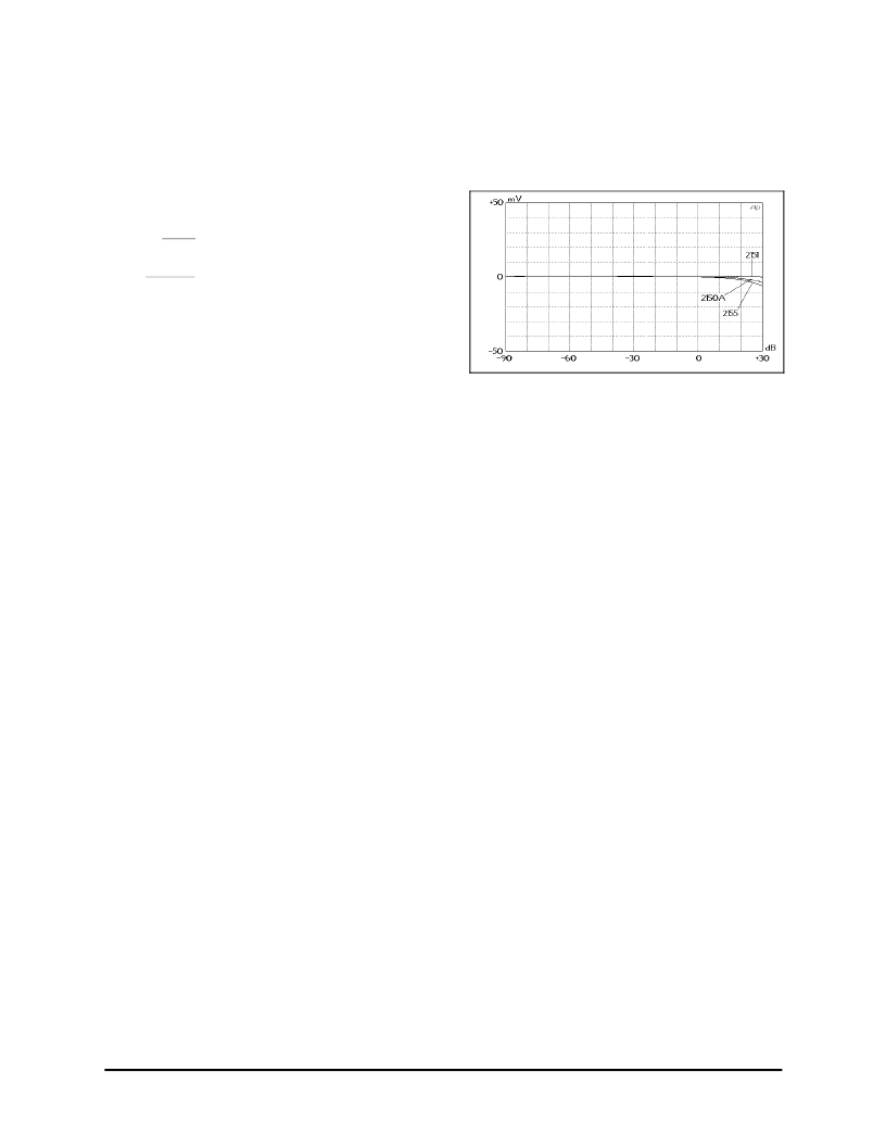
ommended. A plot of typical output offset voltage ver-
sus gain for the circuit of Figure 3 is shown in
Figure 9. (The LF351’s offset was adjusted to 0 V for
this plot.)
Current Programming
The size of the current source at the bottom of the
core (Figure 6, Page 4) is programmed externally via
I
SET
, which is normally determined by a resistor from
pin 5 to V–. The voltage at pin 5 is typically –2.7 V. I
SET
divides into two portions: approximately 400
μ
A is used
for internal biasing, and the rest is available for the
current source at the bottom of the core. I
SET
should
therefore be 400
μ
A larger than the total of the peak
input and output signal currents.
Note that the output impedance of the internal op-
amp is approximately 2 k
, and under peak demands,
the sum of the input and output currents plus I
SET
must be supplied through this impedance, lowering the
voltage available to drive the core. For more informa-
tion, see the
Power Supplies
section on Page 8.
Headroom
Maximum signal currents are also limited by the
logarithmic characteristics of the core transistors. In
the 2150 Series, these devices are specially con-
structed to conform to an ideal log-linear curve over a
wide range of currents, but they reach their limit at ap-
proximately 1 mA. The symptom of failing log confor-
mance is increasing distortion with increasing current
levels. The onset of distortion is gradual at low current
levels, and then more rapid as current becomes high.
Figures 10 through 12 show distortion versus signal
level for the three parts in the 2150 Series for -15 dB,
0 dB, and +15 dB gain. The acceptable distortion will
determine the maximum signal level for a particular
design.
Figure 9. DC Offset Vs. Gain, After Symmetry
Adjustment
THAT Corporation; 734 Forest Street; Marlborough, Massachusetts 01752; USA
Tel: (508) 229-2500; Fax: (508) 229-2590; Web: http:/ / www.thatcorp.com
Page 6
2150 Series IC VCAs
相關(guān)PDF資料 |
PDF描述 |
|---|---|
| THAT2155 | IC Voltage-Controlled Amplifiers |
| THAT2181 | Trimmable IC Voltage Controlled Amplifiers |
| THAT2181A | Trimmable IC Voltage Controlled Amplifiers |
| THAT2181B | Trimmable IC Voltage Controlled Amplifiers |
| THAT2181C | Trimmable IC Voltage Controlled Amplifiers |
相關(guān)代理商/技術(shù)參數(shù) |
參數(shù)描述 |
|---|---|
| THAT2155 | 制造商:未知廠家 制造商全稱:未知廠家 功能描述:IC Voltage-Controlled Amplifiers |
| THAT2180A | 制造商:未知廠家 制造商全稱:未知廠家 功能描述:Pre-Trimmed IC Voltage Controlled Amplifiers |
| THAT2180AL08-U | 制造商:THAT CORPORATION 功能描述:AMP VOLT CONTROLLED PRETRIM 2180 制造商:THAT CORPORATION 功能描述:AMP, VOLT CONTROLLED, PRETRIM, 2180 制造商:THAT CORPORATION 功能描述:AMP, VOLT CONTROLLED, PRETRIM, 2180; IC Function:Voltage Controlled Amplifier; Brief Features:Exponential Gain Control, Wide Gain Range; Supply Voltage Min:-18V; Supply Voltage Max:18V; Operating Temperature Min:0C; Operating ;RoHS Compliant: Yes |
| THAT2180B | 制造商:未知廠家 制造商全稱:未知廠家 功能描述:Pre-Trimmed IC Voltage Controlled Amplifiers |
| THAT2180BL08-U | 制造商:THAT CORPORATION 功能描述:AMP VOLT CONTROLLED PRETRIM 2180 制造商:THAT CORPORATION 功能描述:AMP, VOLT CONTROLLED, PRETRIM, 2180 制造商:THAT CORPORATION 功能描述:AMP, VOLT CONTROLLED, PRETRIM, 2180; IC Function:Voltage Controlled Amplifier; Brief Features:Exponential Gain Control, Wide Gain Range; Supply Voltage Min:-18V; Supply Voltage Max:18V; Operating Temperature Min:0C; Operating ;RoHS Compliant: Yes |
發(fā)布緊急采購,3分鐘左右您將得到回復(fù)。