- 您現(xiàn)在的位置:買賣IC網(wǎng) > PDF目錄373621 > TDA7360 (意法半導(dǎo)體) 22W Bridge / Stereo Audio Amplifier with Clipping Detector(22W橋式立體聲音頻放大器帶限幅檢測(cè)器) PDF資料下載
參數(shù)資料
| 型號(hào): | TDA7360 |
| 廠商: | 意法半導(dǎo)體 |
| 英文描述: | 22W Bridge / Stereo Audio Amplifier with Clipping Detector(22W橋式立體聲音頻放大器帶限幅檢測(cè)器) |
| 中文描述: | 22W橋/立體聲音頻放大器裁剪探測(cè)器(22W橋式立體聲音頻放大器帶限幅檢測(cè)器) |
| 文件頁數(shù): | 9/22頁 |
| 文件大小: | 225K |
| 代理商: | TDA7360 |
AMPLIFIER ORGANIZATION
The TDA7360 has been developedtaking care of
the key concepts of the modern power audio am-
plifier for car radio such as: space and costs sav-
ing due to the minimized external count, excellent
electrical performances, flexibility in use, superior
reliability thanks to a built-in array of protections.
As a result the following performances has been
achieved:
NO NEED OF BOOTSTRAP CAPACITORS
EVEN AT THE HIGHEST OUTPUT POWER
LEVELS
ABSOLUTE STABILITY WITHOUT EXTER-
NAL COMPENSATION THANKS TO THE IN-
NOVATIVE OUT STAGE CONFIGURATION,
ALSO
ALLOWING
CLOSED LOOP LOWER THAN COMPETI-
TORS
LOW GAIN (20dB STEREO FIXED WITHOUT
ANY EXTERNAL COMPONENTS) IN ORDER
INTERNALLY
FIXED
TO MINIMIZE THE OUTPUT NOISE AND OP-
TIMIZE SVR
SILENT MUTE/ST-BY FUNCTION FEATUR-
ING ABSENCE OF POP ON/OFF NOISE
HIGH SVR
STEREO/BRIDGE
OPERATION
ADDITION OF EXTERNAL COMPONENT
AC/DC SHORT CIRCUIT PROTECTION (TO
GND, TO V
S
, ACROSSTHE LOAD)
LOUDSPEAKERPROTECTION
DUMP PROTECTION
ESD PROTECTION
WITHOUT
BLOCKDESCRIPTION
Polarization
The device is organizedwith the gain resistors di-
rectly connected to the signal ground pin i.e. with-
out gain capacitors(fig. 23).
The non inverting inputs of the amplifiers are con-
nected to the SVR pin by means of resistor divid-
ers, equal to the feedback networks. This allows
the outputs to track the SVR pin which is suffi-
ciently slow to avoid audible turn-on and turn-off
transients.
SVR
The voltage ripple on the outputs is equal to the
one on SVR pin: with appropriate selection of
C
SVR
, more than 60dB of ripple rejection can be
obtained.
DelayedTurn-on (muting)
The C
SVR
setsa signal turn-on delay too. A circuit
is included which mutes the device until the volt-
age on SVR pin reaches ~2.5V typ. (fig. 25). The
mute function is obtained by duplicating the input
differential pair (fig. 24): it can be switched to the
signal source or to an internal mute input. This
feature is necessary to prevent transients at the
inputs reaching the loudspeaker(s) immediately
after power-on).
Fig. 25 represents the detailed turn-on transient
with reference to the stereo configuration.
At the power-on the output decoupling capacitors
are charged through an internal path but the de-
vice itself remains switched off (phase 1 of the
representeddiagram).
When the outputs reach the voltage level of about
1V (this means that there is no presence of short
circuits) the device switches on, the SVR capaci-
tor starts charging itself and the output tracks ex-
actlythe SVRpin.
During this phase the device is muted until the
SVR reaches the ”Play” threshold (~2.5V typ.), af-
ter that the music signal starts beingplayed.
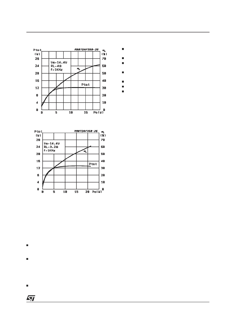
Figure22:
Power Dissipation & Efficiencyvs.
OutputPower (Bridge)
Figure21:
PowerDissipation & Efficiency vs.
OutputPower (Bridge)
TDA7360
9/22
相關(guān)PDF資料 |
PDF描述 |
|---|---|
| TDA7361 | Low Voltage NBFM IF System(低壓NBFM IF系統(tǒng)) |
| TDA7370B | Quad Power Amplifier for Car Radio(用于汽車收音機(jī)的四功率放大器) |
| TDA7370 | QUAD POWER AMPLIFIER FOR CAR RADIO |
| TDA7372A | Power Amplifier for Car Radio(用于汽車收音機(jī)的4×6W功率放大器) |
| TDA7372B | 4 x 6W Power Amplifier for Car Radio(4×6W用于汽車收音機(jī)的功率放大器) |
相關(guān)代理商/技術(shù)參數(shù) |
參數(shù)描述 |
|---|---|
| TDA7360HS | 功能描述:音頻放大器 18V Op 28V DC 36W 50V Supply 5A Output RoHS:否 制造商:STMicroelectronics 產(chǎn)品:General Purpose Audio Amplifiers 輸出類型:Digital 輸出功率: THD + 噪聲: 工作電源電壓:3.3 V 電源電流: 最大功率耗散: 最大工作溫度: 安裝風(fēng)格:SMD/SMT 封裝 / 箱體:TQFP-64 封裝:Reel |
| TDA7361 | 制造商:STMICROELECTRONICS 制造商全稱:STMicroelectronics 功能描述:LOW VOLTAGE NBFM IF SYSTEM |
| TDA7365 | 功能描述:音頻放大器 2X7W Radio Amplifier RoHS:否 制造商:STMicroelectronics 產(chǎn)品:General Purpose Audio Amplifiers 輸出類型:Digital 輸出功率: THD + 噪聲: 工作電源電壓:3.3 V 電源電流: 最大功率耗散: 最大工作溫度: 安裝風(fēng)格:SMD/SMT 封裝 / 箱體:TQFP-64 封裝:Reel |
| TDA7370 | 制造商:STMICROELECTRONICS 制造商全稱:STMicroelectronics 功能描述:QUAD POWER AMPLIFIER FOR CAR RADIO |
| TDA7370B | 制造商:STMICROELECTRONICS 制造商全稱:STMicroelectronics 功能描述:QUAD POWER AMPLIFIER FOR CAR RADIO |
發(fā)布緊急采購,3分鐘左右您將得到回復(fù)。