- 您現(xiàn)在的位置:買(mǎi)賣(mài)IC網(wǎng) > PDF目錄98190 > TDA4470-MSD (ATMEL CORP) SPECIALTY CONSUMER CIRCUIT, PDIP28 PDF資料下載
參數(shù)資料
| 型號(hào): | TDA4470-MSD |
| 廠商: | ATMEL CORP |
| 元件分類: | 消費(fèi)家電 |
| 英文描述: | SPECIALTY CONSUMER CIRCUIT, PDIP28 |
| 封裝: | SHRINK, DIP-28 |
| 文件頁(yè)數(shù): | 17/17頁(yè) |
| 文件大?。?/td> | 116K |
| 代理商: | TDA4470-MSD |
第1頁(yè)第2頁(yè)第3頁(yè)第4頁(yè)第5頁(yè)第6頁(yè)第7頁(yè)第8頁(yè)第9頁(yè)第10頁(yè)第11頁(yè)第12頁(yè)第13頁(yè)第14頁(yè)第15頁(yè)第16頁(yè)當(dāng)前第17頁(yè)

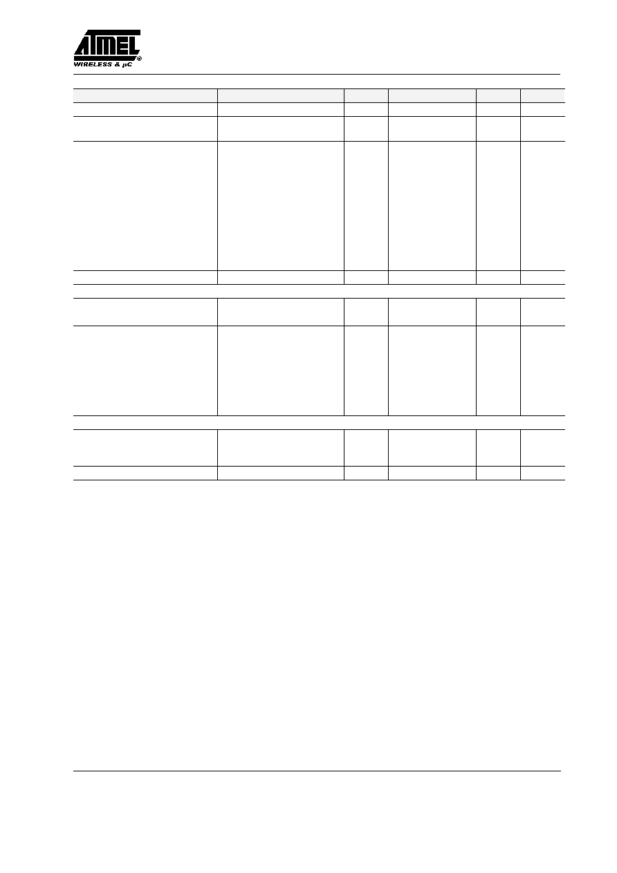
TDA4470
Rev. A4, 23-Feb-01
9 (17)
Unit
Max.
Typ.
Min.
Symbol
Test Conditions / Pins
Parameters
Output resistance
See note 1
Rout
150
W
Sound IF output voltage
(5.5 MHz output voltage)
vin = 10 mV
vout
180
250
350
mVRMS
Weighted signal to noise ratio:
(CCIR 468)
Ref. signal:
vin = 10 mV;
FM dev. =
±27 kHz
fmod = 1 kHz;
tested with the double
FM demod. U2860B;
B/G modulated VIF signal
Black screen: Channel 1/2
Grid pattern: Channel 1/2
Grey screen 50%: Channel
1/2
S/N
60/58
54/52
60/57
dB
Ripple rejection
See note 1, Pin 23/Pin 24
RR
35
dB
AF output-AM
Pin 25
see note 11
DC output voltage
VDC
2.2
V
Output resistance
See note 1
Rout
150
W
AF output voltage
voAF
400
500
630
mVRMS
Total harmonic distortion
m = 54%
fmod = 1 kHz and 12.5 kHz
THD
1
2
%
Signal to noise ratio
Reference: m = 54 %,
fmod = 1 kHz,
22 kHz low pass filter
S/N
65
dB
Ripple rejection
See note 1, Pin 23/Pin 25
RR
28
dB
SIF input selector switch
Pin 3
Control voltage:
input 1 active
input 2 active
See note 12
VSW
2.0
0
VS
0.8
V
Switching current
ISW
±100
mA
Notes
1.)
This parameter is given as an application information and not tested during production.
2.)
In VCR mode the VIF- and SIF path is switched off.
3.)
Adjustment of turn over point (delayed tuner AGC) with external resistor Rtop or external voltage Vtop possible.
4.)
Resonance circuit of VCO (fo = 38.9 MHz): CVCO = 8.2 – 10 pF,
Coil LVCO with unloaded Q-factor Qo
w 60 for an oscillator voltage w 100 mVRMS at Pin 20 – 21
(e.g. TOKO coil 7 KM, 292 XNS - 4051Z)
5.)
The oscillator drift is related to the picture carrier frequency, at external temperature-compensated LC circuit.
6.)
a (1.07) = 20 log (4.43 MHz component/1.07 MHz component); a (1.07) value related to black-white signal
input signal conditions:
picture carrier = 0 dB, colour carrier = –6 dB, sound carrier = –24 dB
7.)
Without external control at Pin 13 the IC automatically operates in mode 1:
negative modulated video-IF signals and FM/NICAM sound signals.
8.)
Without control voltage at Pin 19 falling AFC curve is automatically selected.
9.)
With open circuit at Pin 14 the L’ switch is not active.
10.)
Picture carrier PC = 38.9 MHz; sound carrier SC1 = 33.4 MHz, SC2 = 33.16 MHz;
PC/SC1 =13 dB; PC/SC2 = 20 dB; PC unmodulated (equivalent to sync. peak level).
11.)
Sound carrier SC = 32.4 MHz, modulated with fmod = 1 kHz, m = 54%; vin =10 mV
12.)
Without control voltage at Pin 3 the SIF input 1 is automatically selected.
相關(guān)PDF資料 |
PDF描述 |
|---|---|
| TDA4470-MFLG3 | SPECIALTY CONSUMER CIRCUIT, PDSO28 |
| TDA4470-MFSG3 | SPECIALTY CONSUMER CIRCUIT, PDSO28 |
| TDA4470-MFS | SPECIALTY CONSUMER CIRCUIT, PDSO28 |
| TDA4472-MSD | FM, AUDIO/VIDEO DEMODULATOR, PDIP28 |
| TDA4472-MFLG3 | FM, AUDIO/VIDEO DEMODULATOR, PDSO28 |
相關(guān)代理商/技術(shù)參數(shù) |
參數(shù)描述 |
|---|---|
| TDA4471 | 制造商:TEMIC 制造商全稱:TEMIC Semiconductors 功能描述:Multistandard Video-IF and Quasi Parallel Sound Processing |
| TDA4472 | 制造商:TEMIC 制造商全稱:TEMIC Semiconductors 功能描述:Video-IF and Quasi Parallel Sound Processing |
| TDA4472-A | 制造商:TEMIC 制造商全稱:TEMIC Semiconductors 功能描述:Video-IF (VIF) with FPLL Demodulation and Quasi Parallel Sound (QPS) Processing |
| TDA4472-M | 制造商:TEMIC 制造商全稱:TEMIC Semiconductors 功能描述:Video-IF and Quasi Parallel Sound Processing |
| TDA4472-MFLG3 | 制造商:TEMIC 制造商全稱:TEMIC Semiconductors 功能描述:Video-IF and Quasi Parallel Sound Processing |
發(fā)布緊急采購(gòu),3分鐘左右您將得到回復(fù)。