- 您現(xiàn)在的位置:買賣IC網(wǎng) > PDF目錄98188 > TDA1311AT-T (NXP SEMICONDUCTORS) SERIAL INPUT LOADING, 0.2 us SETTLING TIME, 16-BIT DAC, PDSO8 PDF資料下載
參數(shù)資料
| 型號: | TDA1311AT-T |
| 廠商: | NXP SEMICONDUCTORS |
| 元件分類: | DAC |
| 英文描述: | SERIAL INPUT LOADING, 0.2 us SETTLING TIME, 16-BIT DAC, PDSO8 |
| 封裝: | PLASTIC, SOP-8 |
| 文件頁數(shù): | 2/20頁 |
| 文件大?。?/td> | 104K |
| 代理商: | TDA1311AT-T |

1995 Dec 18
10
Philips Semiconductors
Preliminary specication
Stereo Continuous Calibration DAC
(CC-DAC)
TDA1311A
APPLICATION INFORMATION
Basic application example
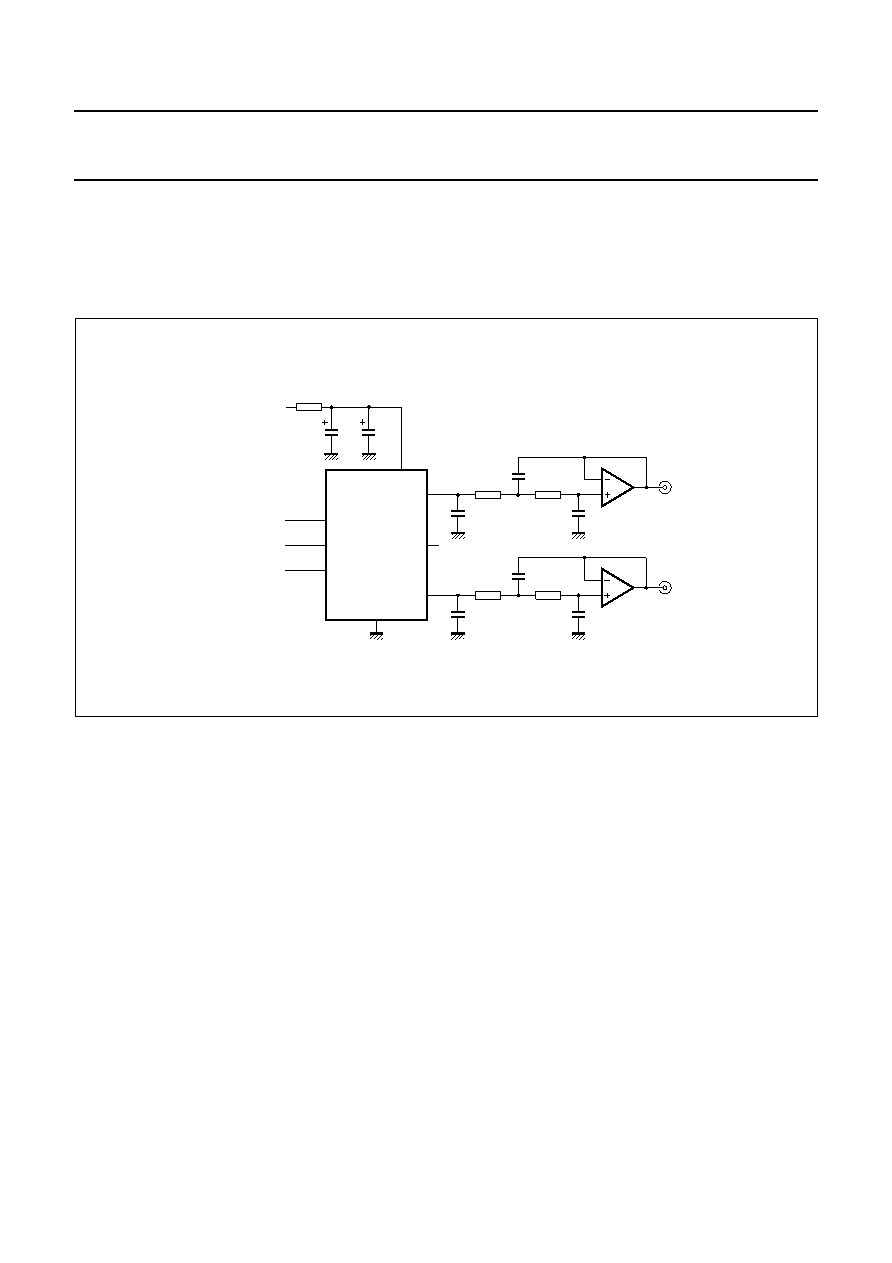
A typical example of a CD-application with the TDA1311A; AT is shown in Fig.6. It features typical decoupling
components and a third-order analog post-filter stage providing a line output.
Fig.6 Example of a 3rd order filter application.
handbook, full pagewidth
100 pF
22 k
420 pF
22 k
2.2 nF
TDA1311A
TDA1311AT
5
8
7
6
4
1
2
3
BCK
WS
DATA
100 pF
22 k
420 pF
22 k
2.2 nF
100
nF
47
F
VDD
10
MBG863
Attention to printed circuit board layout
The TDA1311A and even more so the TDA1311AT offers
great ease in designing-in to printed-circuit boards due to
its small size and low pin count. The TDA1311A; AT being
a mixed-signal IC in CMOS, some attention needs to be
paid to layout and topology of the application PCB.
Following some basic rules will yield the desired
performance. The most important considerations are:
1. Supply: care should be taken to supply the
TDA1311A; AT with a clean, noiseless VDD, for a good
noise performance of the analog parts of the DAC.
Supply purity can easily be achieved by using an
RC-filtered supply.
2. Grounding: preferably a ground plane should be used,
in order to have a low-impedance return available at
any point in the layout. It is advantageous to make a
partitioning of the ground plane according to the nature
of the expected return currents (digital input returns
separate from supply returns and separate from the
analog section).
3. Topology: the capacitor decoupling high-frequency
supply interference from VDD to GND should be placed
as close as is physically possible to the IC body,
ensuring a low-inductance path to ground. The digital
input conductors may be shielded by ground leads
running alongside. The placement of a passive ground
plane underside the entire IC surface gives `free`
additional decoupling from the IC body to ground as
well as providing a shield between the digital input pins
and the analog output pins.
Figure 7 shows recommended layouts for printed-circuit
boards for the SO8 and DIL8 versions respectively. Both
layouts use a single-interconnect layer.
相關(guān)PDF資料 |
PDF描述 |
|---|---|
| TDA1311P | SERIAL INPUT LOADING, 0.2 us SETTLING TIME, 16-BIT DAC, PDIP8 |
| TDA1311T-T | SERIAL INPUT LOADING, 0.2 us SETTLING TIME, 16-BIT DAC, PDSO8 |
| TDA1311T | SERIAL INPUT LOADING, 0.2 us SETTLING TIME, 16-BIT DAC, PDSO8 |
| TDA1311TD-T | SERIAL INPUT LOADING, 0.2 us SETTLING TIME, 16-BIT DAC, PDSO8 |
| TDA1311TD | SERIAL INPUT LOADING, 0.2 us SETTLING TIME, 16-BIT DAC, PDSO8 |
相關(guān)代理商/技術(shù)參數(shù) |
參數(shù)描述 |
|---|---|
| TDA1312 | 制造商:PHILIPS 制造商全稱:NXP Semiconductors 功能描述:Stereo continuous calibration DAC CC-DAC |
| TDA1312A | 制造商:PHILIPS 制造商全稱:NXP Semiconductors 功能描述:Stereo continuous calibration DAC CC-DAC |
| TDA1312AT | 制造商:PHILIPS 制造商全稱:NXP Semiconductors 功能描述:Stereo continuous calibration DAC CC-DAC |
| TDA1313 | 制造商:PHILIPS 制造商全稱:NXP Semiconductors 功能描述:Stereo continuous calibration DAC CC-DAC |
| TDA1313T | 制造商:PHILIPS 制造商全稱:NXP Semiconductors 功能描述:Stereo continuous calibration DAC CC-DAC |
發(fā)布緊急采購,3分鐘左右您將得到回復(fù)。