- 您現(xiàn)在的位置:買賣IC網(wǎng) > PDF目錄385914 > TCM320AC37PT (Texas Instruments, Inc.) VOICE-BAND AUDIO PROCESSORS VBAPE PDF資料下載
參數(shù)資料
| 型號: | TCM320AC37PT |
| 廠商: | Texas Instruments, Inc. |
| 英文描述: | VOICE-BAND AUDIO PROCESSORS VBAPE |
| 中文描述: | 語音頻帶音頻處理器VBAPE |
| 文件頁數(shù): | 10/23頁 |
| 文件大小: | 317K |
| 代理商: | TCM320AC37PT |

TCM320AC36, TCM320AC37
VOICE-BAND AUDIO PROCESSORS (VBAP
)
SLWS003C – MAY 1992 – REVISED APRIL – 1998
10
POST OFFICE BOX 655303
DALLAS, TEXAS 75265
timing requirements
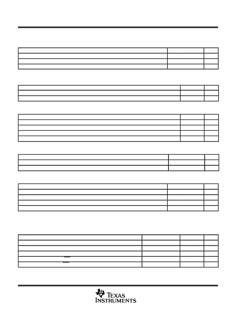
clock timing requirements over recommended ranges of supply voltage and operating free-air temperature
(see Figure 1 through Figure 4)
MIN
NOM
MAX
UNIT
tt
Transition time, CLK and DCLKX/DCLKR
10
ns
Duty cycle, CLK
45%
50%
55%
Duty cycle, DCLKX/DCLKR
All typical values are at VCC = 5 V, TA = 25
°
C.
transmit timing requirements over recommended ranges of supply voltage and operating free-air
temperature, fixed-data-rate mode (see Figure 2)
45%
50%
55%
MIN
MAX
UNIT
tsu(FSX)
th(FSX)
Setup time, FSX high before CLK
↓
Hold time, FSX high after CLK
↓
20
468
ns
20
468
ns
receive timing requirements over recommended ranges of supply voltage and operating free-air
temperature, fixed-data-rate mode (see Figure 1)
MIN
MAX
UNIT
tsu(FSR)
th(FSR)
tsu(DIN)
th(DIN)
Setup time, FSR high before CLK
↓
Hold time, FSR high after CLK
↓
Setup time, DIN high or low before CLK
↓
Hold time, DIN high or low after CLK
↓
20
468
ns
20
468
ns
20
ns
20
ns
transmit timing requirements over recommended ranges of supply voltage and operating free-air
temperature, variable-data-rate mode (see Figure 4)
MIN
MAX
UNIT
tsu(FSX)
th(FSX)
Setup time, FSX high before DCLKX
↓
Hold time, FSX high after DCLKX
↓
40
tc(DCLKX)–40
tc(DCLKX)–35
ns
35
ns
receive timing requirements over recommended ranges of supply voltage and operating free-air
temperature, variable-data-rate mode (see Figure 3)
MIN
MAX
UNIT
tsu(FSR)
th(FSR)
tsu(DIN)
th(DIN)
Setup time, FSR high before DCLKR
↓
Hold time, FSR high after DCLKR
↓
Setup time, DIN high or low before DCLKR
↓
Hold time, DIN high or low after DCLKR
↓
40
ns
35
tc(DCLKR)–35
ns
30
ns
30
ns
switching characteristics
propagation delay times over recommended ranges of operating conditions, fixed-data-rate mode,
C
L
= 0 to 10 pF (see Figure 2)
PARAMETER
TEST CONDITIONS
MIN
MAX
UNIT
tpd1
tpd2
tpd3
tpd4
tpd5
From CLK bit 1 high to DOUT bit 1 valid
35
ns
From CLK high to DOUT valid, bits 2 to n
35
ns
From CLK bit n low to DOUT bit n Hi-Z
30
ns
From CLK bit 1 high to TSX active (low)
Rpullup = 1.24 k
Rpullup = 1.24 k
40
ns
From CLK bit n low to TSX inactive (high)
30
ns
相關(guān)PDF資料 |
PDF描述 |
|---|---|
| TCM320AC54 | MONOLITHIC SERIAL INTERFACE COMBINED PCM CODEC AND FILTER |
| TCM320AC54DW | MONOLITHIC SERIAL INTERFACE COMBINED PCM CODEC AND FILTER |
| TCM320AC54N | MONOLITHIC SERIAL INTERFACE COMBINED PCM CODEC AND FILTER |
| TCM809(中文) | 3-Pin Microcontroller Reset Monitors(3引腳微控制器復(fù)位監(jiān)控器) |
| TCM810(中文) | 3-Pin Microcontroller Reset Monitors(3引腳微控制器復(fù)位監(jiān)控器) |
相關(guān)代理商/技術(shù)參數(shù) |
參數(shù)描述 |
|---|---|
| TCM320AC38 | 制造商:TI 制造商全稱:Texas Instruments 功能描述:VOICE-BAND AUDIO PROCESSORS (VBAPE) |
| TCM320AC39CPT | 制造商:Texas Instruments 功能描述: |
| TCM320AC39IDW | 制造商:Rochester Electronics LLC 功能描述:- Bulk |
| TCM320AC46 | 制造商:TI 制造商全稱:Texas Instruments 功能描述:GEBERAL-PURPOSE AUDIO INTERFACE FOR DSP |
| TCM320AC46CN | 制造商:Rochester Electronics LLC 功能描述:- Bulk |
發(fā)布緊急采購,3分鐘左右您將得到回復(fù)。