- 您現(xiàn)在的位置:買賣IC網(wǎng) > PDF目錄231089 > TC7660MJAG SWITCHED CAPACITOR REGULATOR, 10 kHz SWITCHING FREQ-MAX, CDIP8 PDF資料下載
參數(shù)資料
| 型號(hào): | TC7660MJAG |
| 元件分類: | 穩(wěn)壓器 |
| 英文描述: | SWITCHED CAPACITOR REGULATOR, 10 kHz SWITCHING FREQ-MAX, CDIP8 |
| 封裝: | CERDIP-8 |
| 文件頁(yè)數(shù): | 17/18頁(yè) |
| 文件大小: | 396K |
| 代理商: | TC7660MJAG |
第1頁(yè)第2頁(yè)第3頁(yè)第4頁(yè)第5頁(yè)第6頁(yè)第7頁(yè)第8頁(yè)第9頁(yè)第10頁(yè)第11頁(yè)第12頁(yè)第13頁(yè)第14頁(yè)第15頁(yè)第16頁(yè)當(dāng)前第17頁(yè)第18頁(yè)
TC7660
DS21465B-page 8
2002 Microchip Technology Inc.
5.4
Changing the TC7660 Oscillator
Frequency
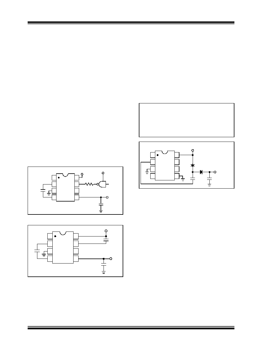
The operating frequency of the TC7660 can be
changed in order to optimize the system performance.
The frequency can be increased by over-driving the
OSC input (Figure 5-4). Any CMOS logic gate can be
utilized in conjunction with a 1 k
series resistor. The
resistor is required to prevent device latch-up. While
TTL level signals can be utilized, an additional 10 k
pull-up resistor to V+ is required. Transitions occur on
the rising edge of the clock input. The resultant output
voltage ripple frequency is one half the clock input.
Higher clock frequencies allow for the use of smaller
pump and reservoir capacitors for a given output volt-
age ripple and droop. Additionally, this allows the
TC7660 to be synchronized to an external clock, elimi-
nating undesirable beat frequencies.
At light loads, lowering the oscillator frequency can
increase the efficiency of the TC7660 (Figure 5-5). By
lowering the oscillator frequency, the switching losses
are reduced. Refer to Figure 2-3 to determine the typi-
cal operating frequency based on the value of the
external capacitor. At lower operating frequencies, it
may be necessary to increase the values of the pump
and reservoir capacitors in order to maintain the
desired output voltage ripple and output impedance.
FIGURE 5-4:
External Clocking.
FIGURE 5-5:
Lowering Oscillator
Frequency.
5.5
Positive Voltage Multiplication
Positive voltage multiplication can be obtained by
employing two external diodes (Figure 5-6). Refer to
the theory of operation of the TC7660 (Section 4.1).
During the half cycle when switch S2 is closed, capaci-
V+ - VF1, where VF1 is the forward voltage drop of diode
D1. During the next half cycle, switch S1 is closed, shift-
ing the reference of capacitor C1 from GND to V+. The
energy in capacitor C1 is transferred to capacitor C2
through diode D2, producing an output voltage of
approximately:
EQUATION
FIGURE 5-6:
Positive Voltage Multiplier.
5.6
Combined Negative Voltage
Conversion and Positive Supply
Multiplication
Simultaneous voltage inversion and positive voltage
multiplication can be obtained (Figure 5-7). Capacitors
C1 and C3 perform the voltage inversion, while capaci-
tors C2 and C4, plus the two diodes, perform the posi-
tive voltage multiplication. Capacitors C1 and C2 are
the pump capacitors, while capacitors C3 and C4 are
the reservoir capacitors for their respective functions.
Both functions utilize the same switches of the TC7660.
As a result, if either output is loaded, both outputs will
drop towards GND.
CMOS
GATE
1k
VOUT
“1”
+
V+
+
1
2
3
4
8
7
6
5
TC7660
10 F
V+
VOUT
+
1
2
3
4
8
7
6
5
TC7660
C1
C2
V+
COSC
VOUT
2V
+
×
VF1 VF2
+
()
–
=
where:
VF1 is the forward voltage drop of diode D1
and
VF2 is the forward voltage drop of diode D2.
+
C2
D1
D2
+
C1
VOUT =
1
2
3
4
8
7
6
5
TC7660
V+
(2 V+) - (2 VF)
相關(guān)PDF資料 |
PDF描述 |
|---|---|
| TPS65200YFFT | 1-CHANNEL POWER SUPPLY SUPPORT CKT, BGA36 |
| TC151A3318EOA713 | 0.25 A SWITCHING REGULATOR, 50 kHz SWITCHING FREQ-MAX, PDSO8 |
| TC151A4939EOA713 | 0.25 A SWITCHING REGULATOR, 50 kHz SWITCHING FREQ-MAX, PDSO8 |
| TC161A5917EOA723 | 0.25 A SWITCHING REGULATOR, 100 kHz SWITCHING FREQ-MAX, PDSO8 |
| TC161B1524EOA723 | 0.25 A SWITCHING REGULATOR, 100 kHz SWITCHING FREQ-MAX, PDSO8 |
相關(guān)代理商/技術(shù)參數(shù) |
參數(shù)描述 |
|---|---|
| TC7660MOA | 制造商:MICROCHIP 制造商全稱:Microchip Technology 功能描述:Charge Pump DC-to-DC Voltage Converter |
| TC7660MOA713 | 制造商:MICROCHIP 制造商全稱:Microchip Technology 功能描述:Charge Pump DC-to-DC Voltage Converter |
| TC7660MPA | 制造商:MICROCHIP 制造商全稱:Microchip Technology 功能描述:Charge Pump DC-to-DC Voltage Converter |
| TC7660S | 制造商:MICROCHIP 制造商全稱:Microchip Technology 功能描述:SUPER CHARGE PUMP DC-TO-DC VOLTAGE CONVERTER |
| TC7660SCOA | 功能描述:電荷泵 High Voltage RoHS:否 制造商:Maxim Integrated 功能:Inverting, Step Up 輸出電壓:- 1.5 V to - 5.5 V, 3 V to 11 V 輸出電流:100 mA 電源電流:1 mA 最大工作溫度:+ 70 C 封裝 / 箱體:SOIC-8 Narrow 封裝:Tube |
發(fā)布緊急采購(gòu),3分鐘左右您將得到回復(fù)。