- 您現(xiàn)在的位置:買賣IC網(wǎng) > PDF目錄383929 > TC4422VMF713 (Microchip Technology Inc.) 9A High-Speed MOSFET Drivers PDF資料下載
參數(shù)資料
| 型號(hào): | TC4422VMF713 |
| 廠商: | Microchip Technology Inc. |
| 英文描述: | 9A High-Speed MOSFET Drivers |
| 中文描述: | 第9A高速M(fèi)OSFET驅(qū)動(dòng)器 |
| 文件頁(yè)數(shù): | 3/18頁(yè) |
| 文件大小: | 272K |
| 代理商: | TC4422VMF713 |
第1頁(yè)第2頁(yè)當(dāng)前第3頁(yè)第4頁(yè)第5頁(yè)第6頁(yè)第7頁(yè)第8頁(yè)第9頁(yè)第10頁(yè)第11頁(yè)第12頁(yè)第13頁(yè)第14頁(yè)第15頁(yè)第16頁(yè)第17頁(yè)第18頁(yè)
2004 Microchip Technology Inc.
DS21420D-page 3
TC4421/TC4422
1.0
ELECTRICAL
CHARACTERISTICS
Absolute Maximum Ratings
Supply Voltage.....................................................+20V
Input Voltage....................(V
DD
+ 0.3V) to (GND – 5V)
Input Current (V
IN
> V
DD
)...................................50 mA
Package Power Dissipation (T
A
≤
70°C)
5-Pin TO-220....................................................1.6W
DFN..............................................................
Note 2
PDIP............................................................730 mW
SOIC............................................................750 mW
Package Power Dissipation (T
A
≤
25°C)
5-Pin TO-220 (With Heatsink) ........................12.5W
Thermal Impedances (To Case)
5-Pin TO-220 R
θ
J-C
......................................10°C/W
Stresses above those listed under “Absolute Maximum
Ratings” may cause permanent damage to the device. These
are stress ratings only and functional operation of the device
at these or any other conditions above those indicated in the
operation sections of the specifications is not implied.
Exposure to Absolute Maximum Rating conditions for
extended periods may affect device reliability.
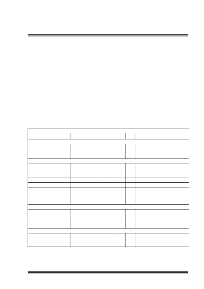
DC CHARACTERISTICS
Electrical Specifications:
Unless otherwise noted, T
A
= +25°C with 4.5V
≤
V
DD
≤
18V.
Parameters
Sym
Min
Typ
Max
Units
Conditions
Input
Logic ‘
1
’, High Input Voltage
Logic ‘
0
’, Low Input Voltage
Input Current
Output
High Output Voltage
Low Output Voltage
Output Resistance, High
Output Resistance, Low
Peak Output Current
Continuous Output Current
V
IH
V
IL
I
IN
2.4
—
–10
1.8
1.3
—
—
0.8
+10
V
V
μA
0V
≤
V
IN
≤
V
DD
V
OH
V
OL
R
OH
R
OL
I
PK
I
DC
V
DD
– 0.025
—
—
—
—
2
—
—
1.4
0.9
9.0
—
—
V
V
A
A
DC TEST
DC TEST
I
OUT
= 10 mA, V
DD
= 18V
I
OUT
= 10 mA, V
DD
= 18V
V
DD
= 18V
10V
≤
V
DD
≤
18V, T
A
= +25°C
(
TC4421/TC4422
CAT only)
(Note 3)
Duty cycle
≤
2%, t
≤
300 μsec
0.025
—
1.7
—
—
Latch-Up Protection
Withstand Reverse Current
Switching Time
(Note 1)
Rise Time
Fall Time
Delay Time
Delay Time
Power Supply
Power Supply Current
I
REV
—
>1.5
—
A
t
R
t
F
t
D1
t
D2
—
—
—
—
60
60
30
33
75
75
60
60
ns
ns
ns
ns
Figure 4-1
, C
L
= 10,000 pF
Figure 4-1
, C
L
= 10,000 pF
Figure 4-1
Figure 4-1
I
S
—
—
4.5
0.2
55
—
1.5
150
18
mA
μA
V
V
IN
= 3V
V
IN
= 0V
Operating Input Voltage
Note 1:
Switching times ensured by design.
2:
Package power dissipation is dependent on the copper pad area on the PCB.
3:
Tested during characterization, not production tested.
V
DD
相關(guān)PDF資料 |
PDF描述 |
|---|---|
| TC4422VPA | 9A High-Speed MOSFET Drivers |
| TC4422VSM.SM713 | 9A High-Speed MOSFET Drivers |
| TC4423CG | 3A Dual High-Speed Power MOSFET Drivers |
| TC4423CMF | 3A Dual High-Speed Power MOSFET Drivers |
| TC4423CMF713 | 3A Dual High-Speed Power MOSFET Drivers |
相關(guān)代理商/技術(shù)參數(shù) |
參數(shù)描述 |
|---|---|
| TC4422VPA | 功能描述:功率驅(qū)動(dòng)器IC 9A Sngl RoHS:否 制造商:Micrel 產(chǎn)品:MOSFET Gate Drivers 類型:Low Cost High or Low Side MOSFET Driver 上升時(shí)間: 下降時(shí)間: 電源電壓-最大:30 V 電源電壓-最小:2.75 V 電源電流: 最大功率耗散: 最大工作溫度:+ 85 C 安裝風(fēng)格:SMD/SMT 封裝 / 箱體:SOIC-8 封裝:Tube |
| TC4422VSM.SM713 | 制造商:MICROCHIP 制造商全稱:Microchip Technology 功能描述:9A High-Speed MOSFET Drivers |
| TC4423 | 制造商:MICROCHIP 制造商全稱:Microchip Technology 功能描述:3A DUAL HIGH-SPEED POWER MOSFET DRIVERS |
| TC4423_04 | 制造商:MICROCHIP 制造商全稱:Microchip Technology 功能描述:3A Dual High-Speed Power MOSFET Drivers |
| TC4423_13 | 制造商:MICROCHIP 制造商全稱:Microchip Technology 功能描述:3A Dual High-Speed Power MOSFET Drivers |
發(fā)布緊急采購(gòu),3分鐘左右您將得到回復(fù)。