- 您現(xiàn)在的位置:買(mǎi)賣(mài)IC網(wǎng) > PDF目錄373558 > TAR8D05K (Toshiba Corporation) Dual Low-Dropout Regulator PDF資料下載
參數(shù)資料
| 型號(hào): | TAR8D05K |
| 廠(chǎng)商: | Toshiba Corporation |
| 英文描述: | Dual Low-Dropout Regulator |
| 中文描述: | 雙低壓差穩(wěn)壓器 |
| 文件頁(yè)數(shù): | 2/7頁(yè) |
| 文件大小: | 168K |
| 代理商: | TAR8D05K |
TAR8D05K
2007-11-01
2
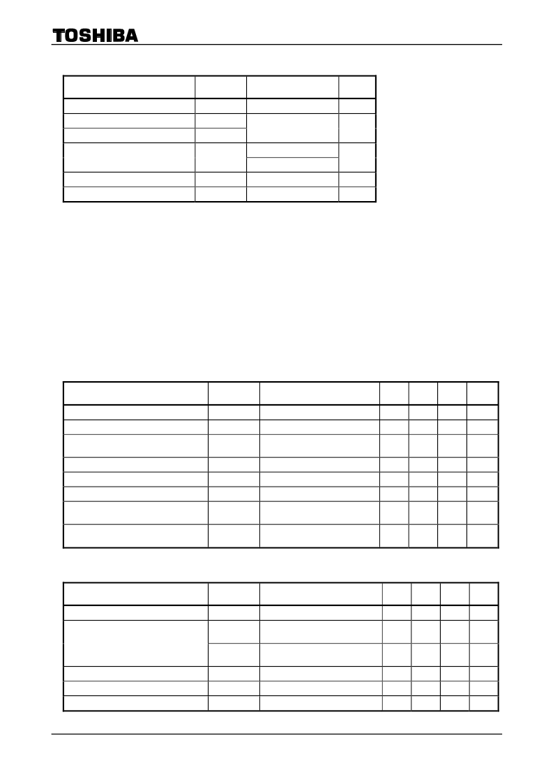
Absolute Maximum Ratings
(Ta
=
25°C)
Characteristics
Symbol
Rating
Unit
Supply Voltage
V
IN
15
V
Output Current (V
OUT
(A) )
I
OUT
(A)
Output Current (V
OUT
(B) )
I
OUT
(B)
100
mA
200
(Note 1)
Power Dissipation
P
D
400
(Note 2)
mW
Operation Temp Range
T
opr
40~85
°C
Storage Temp Range
T
stg
55~150
°C
Note:
Using continuously under heavy loads (e.g. the application of high temperature/current/voltage and the
significant change in temperature, etc.) may cause this product to decrease in the reliability significantly
even if the operating conditions (i.e. operating temperature/current/voltage, etc.) are within the absolute
maximum ratings and the operating ranges.
Please design the appropriate reliability upon reviewing the Toshiba Semiconductor Reliability Handbook
(“Handling Precautions”/“Derating Concept and Methods”) and individual reliability data (i.e. reliability test
report and estimated failure rate, etc).
Note 1: Unit Rating
Note 2: Mounted on a glass epoxy circuit board of 30 mm
×
30 mm Pad dimansion of 70 mm
2
Electrical Characteristics
(unless otherwise specified, V
IN
=
V
OUT
+
1 V, I
OUT
=
30 mA, C
IN
=
1
μ
F, C
OUT
=
10
μ
F, C
NOISE
=
0.01
μ
F, T
j
=
25°C)
2.8 V output Characteristics
(V
OUT
(A), V
OUT
(B) )
Characteristics
Symbol
Test Condition
Min
Typ
Max
Unit
Output Voltage
V
OUT
I
OUT
=
30 mA
2.73
2.8
2.87
V
Dropout Voltage
V
IN
-V
OUT
I
OUT
=
30 mA
120
180
Input Voltatge
V
IN
V
OUT
+
0.18 V
15
V
Load Regulation
Reg
load
I
OUT
=
0 mA~30 mA
2
12
mV
Line Reguration
Reg
line
V
IN
=
3.8 V~15.0 V
3
15
mV
Temp. Coeffcient
T
CVO
Ta
=
40
°
C~85
°
C
100
ppm/
°
C
Ripple Rejection
R.R
I
OUT
=
10 mA, f
=
1 kHz,
V
Ripple
=
500 mV
p-p
, Ta
=
25
°
C
70
dB
Output Noise Voltage
V
NO
I
OUT
=
10 mA,
10 Hz
<
f
<
10 kHz, Ta
=
25
°
C
30
μ
V
rms
Common Characteristics
Characteristics
Symbol
Test Condition
Min
Typ
Max
Unit
Stand-by Current
I
B (OFF)
V
CT
=
0 V
1
μ
A
I
B1
I
OUT
(A)
=
0 mA,
I
OUT
(B)
=
0 mA
350
700
μ
A
Quiescent Current
I
B2
I
OUT
(A)
=
30 mA,
I
OUT
(B)
=
30 mA
850
1800
μ
A
Control Voltage (ON)
V
CT (ON)
1.5
V
IN
V
Control Voltage (OFF)
V
CT (OFF)
0.4
V
Control Input Current
I
CT
V
CT
=
1.5 V (output ON)
15
μ
A
相關(guān)PDF資料 |
PDF描述 |
|---|---|
| TAR8D06K | Dual Low-Dropout Regulator |
| TAR8D08K | Dual Low-Dropout Regulator |
| TAR8H01K | Dual Low-Dropout Regulator |
| TAR8H02K | Dual Low-Dropout Regulator |
| TAR8H03K | Dual Low-Dropout Regulator |
相關(guān)代理商/技術(shù)參數(shù) |
參數(shù)描述 |
|---|---|
| TAR8D06K | 制造商:TOSHIBA 制造商全稱(chēng):Toshiba Semiconductor 功能描述:Dual Low-Dropout Regulator |
| TAR8D08K | 制造商:TOSHIBA 制造商全稱(chēng):Toshiba Semiconductor 功能描述:Dual Low-Dropout Regulator |
| TAR8H01K | 制造商:TOSHIBA 制造商全稱(chēng):Toshiba Semiconductor 功能描述:Dual Low-Dropout Regulator |
| TAR8H02K | 制造商:TOSHIBA 制造商全稱(chēng):Toshiba Semiconductor 功能描述:Dual Low-Dropout Regulator |
| TAR8H03K | 制造商:TOSHIBA 制造商全稱(chēng):Toshiba Semiconductor 功能描述:Dual Low-Dropout Regulator |
發(fā)布緊急采購(gòu),3分鐘左右您將得到回復(fù)。