- 您現(xiàn)在的位置:買賣IC網(wǎng) > PDF目錄373555 > TA8696 (Toshiba Corporation) MINIATURE POWER RELAY PDF資料下載
參數(shù)資料
| 型號: | TA8696 |
| 廠商: | Toshiba Corporation |
| 英文描述: | MINIATURE POWER RELAY |
| 中文描述: | 東芝雙極線性集成電路硅單片 |
| 文件頁數(shù): | 6/12頁 |
| 文件大小: | 210K |
| 代理商: | TA8696 |
TA8696F
2002-02-13
6
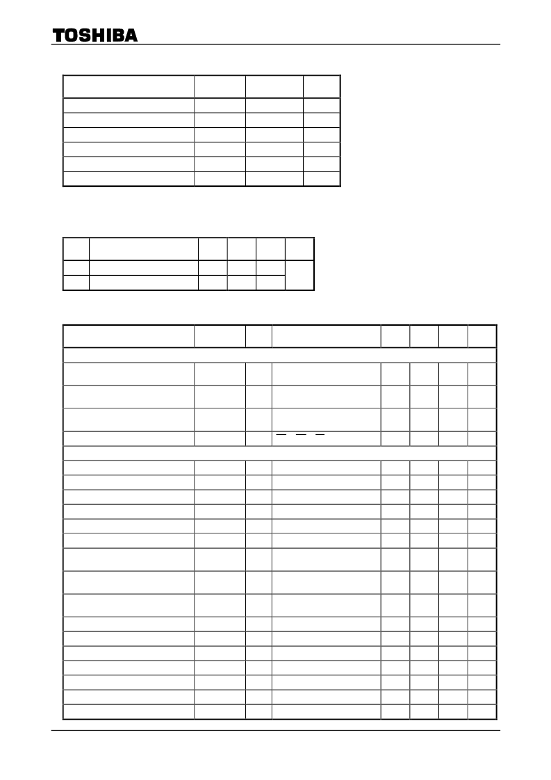
Maximum Ratings
(Ta 25°C)
Characteristics
Symbol
Rating
Unit
Power supply voltage
L.V
CC
8
V
Power supply voltage
H.V
CC
14.5
V
Power dissipation
P
D
890
mW
Power dissipation lowering rate
ja
7.2
mW/°C
Operating temperature
T
opr
20 to 75
°C
Storage temperature
T
stg
55 to 150
°C
Note 2: When the IC is operated at 25°C or higher, reduce power dissipation by 12.8 mW per degree.
Recommended Power Supply Voltage
Pin
No.
Pin Name
Min
Typ.
Max
Unit
15
L.V
CC
3.3
5.0
7.5
26
H.V
CC
10.0
13.0
14.0
V
Electrical Characteristics
(unless otherwise specified, V
CC
4 V, Ta 25°C)
Characteristics
Symbol
Test
Circuit
Test Condition
Min
Typ.
Max
Unit
[1] Operating range
Primary color input white signal level
2
The same conditions are given
to R/G/B-axis.
1.6
V
Primary color input black signal level
2
The same conditions are given
to R/G/B-axis.
0.9
V
CH indication signal level
2
The same conditions are given
to R/G/B-axis.
3
5
5.5
V
Timing pulse level
2
HD
,
VD
,
LD
3
5
5.5
V
[2] Electrical characteristics
Operating power supply current (1)
2
Pin 15.L.V
CC
4 V No load.
5.8
8.4
10.9
mA
Operating power supply current (2)
2
Pin 26.H.V
CC
13 V No load.
3.2
4.6
6.0
mA
Input signal dynamic range
2
1.2
1.4
1.6
V
Input signal pin resistor
R
IN
2
10.5
14.0
17.5
k
Input signal pin capacity
C
IN
2
1
3
pF
Black signal level off-set
2
off-set open
100
200
mV
Black signal level off-set difference in
the axes
2
50
100
mV
Black signal level off-set adjustment
amount
2
0.3
V
Black signal level off-set adjustment
sensitivity
2
300
mV/V
Input off-set elimination capacity
2
20
26
dB
Off-set cancel difference in the axes
2
50
mV
Typical gain
2
Drive adjustment open
9.4
12.4
15.4
dB
Typical gain difference in the axes
2
Drive adjustment open
0.5
dB
Typical gain difference in the polarity
2
Drive adjustment open
0.5
dB
Maximum gain
2
15.4
18.4
dB
Minimum gain
2
20
10
dB
相關(guān)PDF資料 |
PDF描述 |
|---|---|
| TA8696F | TOSHIBA Bipolar Linear Integrated Circuit Silicon Monolithic |
| TA8703 | QUASI-SIF SYSTEM FOR TV |
| TA8703S | QUASI-SIF SYSTEM FOR TV |
| TA8710 | SIF CONVERTER FOR TV AND VTR |
| TA8710S | DIODE - ULTRAFAST 600V 1A SMA (0.115 X 0.220) |
相關(guān)代理商/技術(shù)參數(shù) |
參數(shù)描述 |
|---|---|
| TA8696F | 制造商:TOSHIBA 制造商全稱:Toshiba Semiconductor 功能描述:TOSHIBA Bipolar Linear Integrated Circuit Silicon Monolithic |
| TA-8700 | 制造商:FLORIDA MISC. 功能描述: |
| TA8700AN | 制造商:TOSHIBA 制造商全稱:Toshiba Semiconductor 功能描述:PIF/SIF IC FOR TV/VTR |
| TA8701AN | 制造商:TOSHIBA 制造商全稱:Toshiba Semiconductor 功能描述:PIF/SIF + ATT IC FOR TV/VTR |
| TA8703 | 制造商:TOSHIBA 制造商全稱:Toshiba Semiconductor 功能描述:QUASI-SIF SYSTEM FOR TV |
發(fā)布緊急采購,3分鐘左右您將得到回復(fù)。