- 您現(xiàn)在的位置:買賣IC網(wǎng) > PDF目錄98151 > TA1276AF SPECIALTY CONSUMER CIRCUIT, PQFP80 PDF資料下載
參數(shù)資料
| 型號: | TA1276AF |
| 元件分類: | 消費家電 |
| 英文描述: | SPECIALTY CONSUMER CIRCUIT, PQFP80 |
| 封裝: | 14 X 20 MM, 0.80 MM PITCH, PLASTIC, QFP-80 |
| 文件頁數(shù): | 55/83頁 |
| 文件大?。?/td> | 1585K |
| 代理商: | TA1276AF |
第1頁第2頁第3頁第4頁第5頁第6頁第7頁第8頁第9頁第10頁第11頁第12頁第13頁第14頁第15頁第16頁第17頁第18頁第19頁第20頁第21頁第22頁第23頁第24頁第25頁第26頁第27頁第28頁第29頁第30頁第31頁第32頁第33頁第34頁第35頁第36頁第37頁第38頁第39頁第40頁第41頁第42頁第43頁第44頁第45頁第46頁第47頁第48頁第49頁第50頁第51頁第52頁第53頁第54頁當(dāng)前第55頁第56頁第57頁第58頁第59頁第60頁第61頁第62頁第63頁第64頁第65頁第66頁第67頁第68頁第69頁第70頁第71頁第72頁第73頁第74頁第75頁第76頁第77頁第78頁第79頁第80頁第81頁第82頁第83頁
TA1276AF
2002-01-29
59
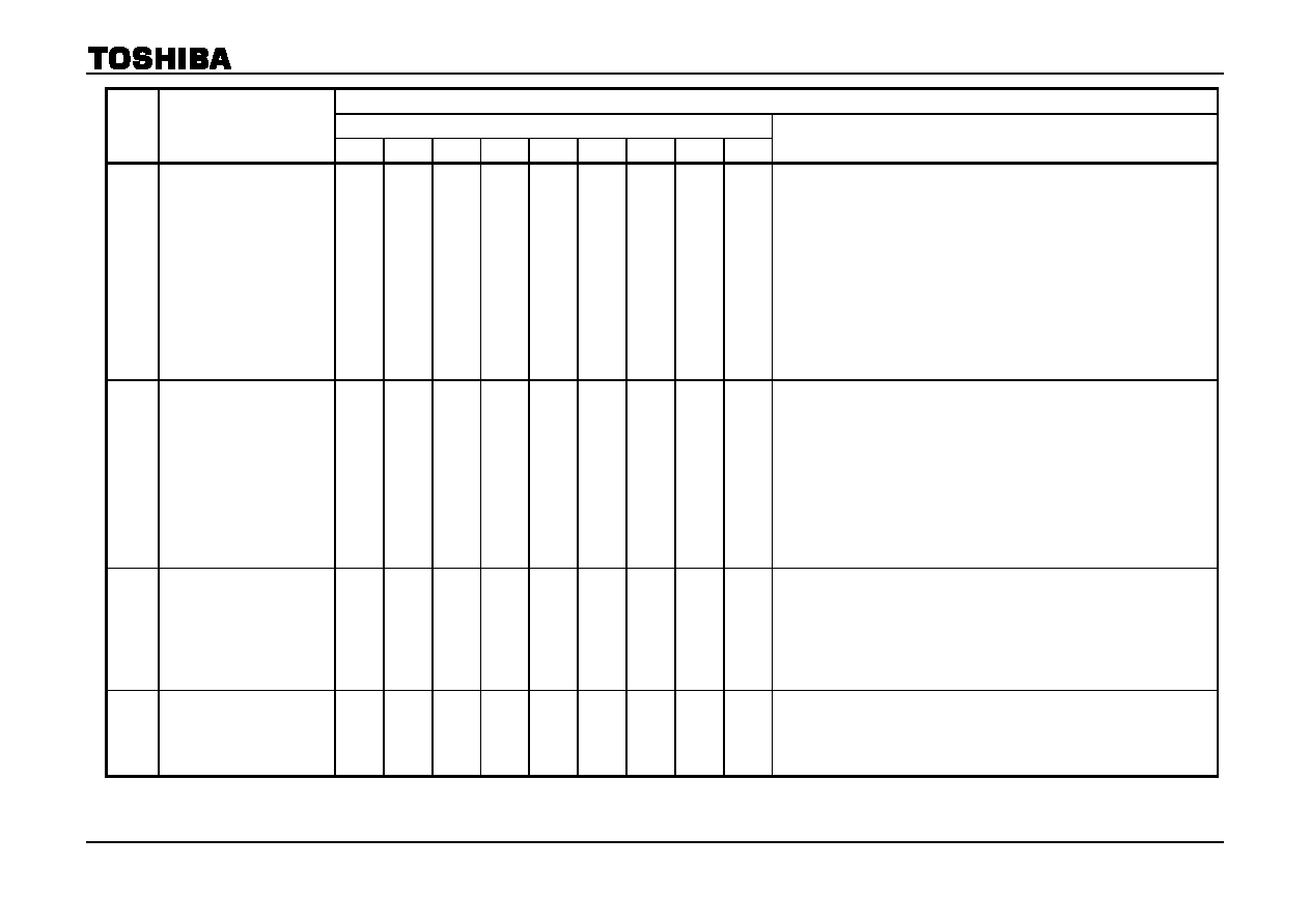
Test Conditions (unless otherwise stated, VCC1 = 5 V, VCC2/VCC3/DEF VCC = 9 V, Ta = 25 ± 3°C)
Switching Mode
Note
Parameter
SW33
SW34
SW35
SW37
SW38
SW39
SW51
SW52
SW53
Test Conditions
T27
Analog OSD Gain
↑
A
or
B
A
or
B
A
or
B
↑
1)
Input signal 1 (f0 = 100 kHz, picture period amplitude = 0.2 Vp-p) to pin 78
and adjust the drive adjustment data so that the picture period amplitudes
of pins 13 and 15 are equal to that of pin 11.
2)
Apply 5 V from an external power supply to pin 21.
3)
Input signal 1 (f0 = 100 kHz, picture period amplitude = 0.2 Vp-p) to pin 18.
4)
Measure the picture period amplitude of pin 11. (V43R)
5)
As in steps 3) and 4) above, input to pin 19 and measure pin 13, then input
to pin 20 and measure pin 15. (V42G, V41B)
6)
GOSDR = V43R/0.2
GOSDG = V42G/0.2
GOSDB = V41B/0.2
T28
Analog OSD White Peak Slice
Level
A
B
A
1)
Repeat step 1) of T27.
2)
Apply 5 V from an external power supply to pin 21.
3)
Apply external voltage to pin 18, increase the voltage gradually from 0.0 V,
and measure the picture period amplitude voltage when pin 11 is clipped.
(VOSD1R)
4)
As in step 3) above, input to pin 19 and measure pin 13. Input to pin 20
and measure pin 15.
5)
Set the subaddress (10) data to (04) and repeat the measurements in
steps 3) and 4).
(VOSD2R, VOSD2G, VOSD2B)
T29
Analog OSD Black Peak
Limiter Level
↑
1)
Repeat step 1) of T27.
2)
Apply 5 V from an external power supply to pin 21.
3)
Apply external voltage to pin 18, decrease the voltage gradually from 4.5
V, and measure the voltage when pin 11 is clipped.
4)
As in step 3) above, input to pin 19 and measure pin 13. Input to pin 20
and measure pin 15.
T30
Analog OSD Output DC
Voltage
↑
1)
Repeat step 1) of T27.
2)
Apply 5 V from an external power supply to pin 21.
3)
Measure the picture period voltages of pins 11, 13, and 15.
(VOSDDCR, VOSDDCG, VOSDDCB)
相關(guān)PDF資料 |
PDF描述 |
|---|---|
| TA1281FA | 3-BAND, VIDEO TUNER, PDSO16 |
| TA1281F | 3-BAND, VIDEO TUNER, PDSO16 |
| TA1290FN | SPECIALTY CONSUMER CIRCUIT, PDSO16 |
| TA1291N | SPECIALTY CONSUMER CIRCUIT, PDIP56 |
| TA1291N | SPECIALTY CONSUMER CIRCUIT, PDIP56 |
相關(guān)代理商/技術(shù)參數(shù) |
參數(shù)描述 |
|---|---|
| TA1276AFG | 制造商:TOSHIBA 制造商全稱:Toshiba Semiconductor 功能描述:PAL/NTSC Video Chroma And Deflection IC For CTV |
| TA1276AN | 制造商:Panasonic Industrial Company 功能描述:IC 制造商:Toshiba America Electronic Components 功能描述:Tv/Video Signal Proce or Toshiba IC 56-Pin DIP-S |
| TA1281 | 制造商:TOSHIBA 制造商全稱:Toshiba Semiconductor 功能描述:UHF/VHF TUNER IC |
| TA1281F | 制造商:TOSHIBA 制造商全稱:Toshiba Semiconductor 功能描述:UHF/VHF TUNER IC |
| TA1281FA | 制造商:TOSHIBA 制造商全稱:Toshiba Semiconductor 功能描述:UHF/VHF TUNER IC |
發(fā)布緊急采購,3分鐘左右您將得到回復(fù)。