- 您現(xiàn)在的位置:買賣IC網(wǎng) > PDF目錄272328 > T80C31-20R (ATMEL CORP) 8-BIT, 20 MHz, MICROCONTROLLER, PQFP44 PDF資料下載
參數(shù)資料
| 型號: | T80C31-20R |
| 廠商: | ATMEL CORP |
| 元件分類: | 微控制器/微處理器 |
| 英文描述: | 8-BIT, 20 MHz, MICROCONTROLLER, PQFP44 |
| 封裝: | 1 MM HEIGHT, QFP-44 |
| 文件頁數(shù): | 91/170頁 |
| 文件大?。?/td> | 4133K |
| 代理商: | T80C31-20R |
第1頁第2頁第3頁第4頁第5頁第6頁第7頁第8頁第9頁第10頁第11頁第12頁第13頁第14頁第15頁第16頁第17頁第18頁第19頁第20頁第21頁第22頁第23頁第24頁第25頁第26頁第27頁第28頁第29頁第30頁第31頁第32頁第33頁第34頁第35頁第36頁第37頁第38頁第39頁第40頁第41頁第42頁第43頁第44頁第45頁第46頁第47頁第48頁第49頁第50頁第51頁第52頁第53頁第54頁第55頁第56頁第57頁第58頁第59頁第60頁第61頁第62頁第63頁第64頁第65頁第66頁第67頁第68頁第69頁第70頁第71頁第72頁第73頁第74頁第75頁第76頁第77頁第78頁第79頁第80頁第81頁第82頁第83頁第84頁第85頁第86頁第87頁第88頁第89頁第90頁當(dāng)前第91頁第92頁第93頁第94頁第95頁第96頁第97頁第98頁第99頁第100頁第101頁第102頁第103頁第104頁第105頁第106頁第107頁第108頁第109頁第110頁第111頁第112頁第113頁第114頁第115頁第116頁第117頁第118頁第119頁第120頁第121頁第122頁第123頁第124頁第125頁第126頁第127頁第128頁第129頁第130頁第131頁第132頁第133頁第134頁第135頁第136頁第137頁第138頁第139頁第140頁第141頁第142頁第143頁第144頁第145頁第146頁第147頁第148頁第149頁第150頁第151頁第152頁第153頁第154頁第155頁第156頁第157頁第158頁第159頁第160頁第161頁第162頁第163頁第164頁第165頁第166頁第167頁第168頁第169頁第170頁
27
ATtiny4/5/9/10 [DATASHEET]
8127F–AVR–02/2013
8.
System Control and Reset
8.1
Resetting the AVR
During reset, all I/O registers are set to their initial values, and the program starts execution from the Reset Vector.
The instruction placed at the Reset Vector must be a RJMP – Relative Jump – instruction to the reset handling rou-
tine. If the program never enables an interrupt source, the interrupt vectors are not used, and regular program code
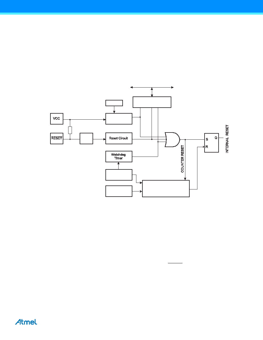
can be placed at these locations. The circuit diagram in Figure 8-1 shows the reset logic. Electrical parameters of
the reset circuitry are defined in section “System and Reset Characteristics” on page 118.
Figure 8-1.
Reset Logic
The I/O ports of the AVR are immediately reset to their initial state when a reset source goes active. This does not
require any clock source to be running.
After all reset sources have gone inactive, a delay counter is invoked, stretching the internal reset. This allows the
power to reach a stable level before normal operation starts. The start up sequence is described in “Starting from
8.2
Reset Sources
The ATtiny4/5/9/10 have three sources of reset:
Power-on Reset. The MCU is reset when the supply voltage is below the Power-on Reset threshold (V
POT)
External Reset. The MCU is reset when a low level is present on the RESET pin for longer than the minimum
pulse length
Watchdog Reset. The MCU is reset when the Watchdog Timer period expires and the Watchdog is enabled
8.2.1
Power-on Reset
A Power-on Reset (POR) pulse is generated by an on-chip detection circuit. The detection level is defined in sec-
tion “System and Reset Characteristics” on page 118. The POR is activated whenever V
CC is below the detection
level. The POR circuit can be used to trigger the Start-up Reset, as well as to detect a failure in supply voltage.
Reset Flag Register
(RSTFLR)
Delay Counters
CK
TIMEOUT
WDRF
EXTRF
PORF
DATA BUS
Clock
Generator
SPIKE
FILTER
Pull-up Resistor
Watchdog
Oscillator
Power-on Reset
Circuit
VLM
相關(guān)PDF資料 |
PDF描述 |
|---|---|
| T80C31-20D | 8-BIT, 20 MHz, MICROCONTROLLER, PQFP44 |
| TSC87C52-25MIMQ | 8-BIT, OTPROM, 25 MHz, MICROCONTROLLER, CQCC44 |
| TSC87C52-25MJ | 8-BIT, UVPROM, 25 MHz, MICROCONTROLLER, CDIP40 |
| TSC87C52-25MK/883 | 8-BIT, UVPROM, 25 MHz, MICROCONTROLLER, CQCC44 |
| TMP87CH00DF | 8-BIT, MROM, 8 MHz, MICROCONTROLLER, PQFP64 |
相關(guān)代理商/技術(shù)參數(shù) |
參數(shù)描述 |
|---|---|
| T80C31-25 | 制造商:未知廠家 制造商全稱:未知廠家 功能描述:8-Bit Microcontroller |
| T80C31-30 | 制造商:未知廠家 制造商全稱:未知廠家 功能描述:8-Bit Microcontroller |
| T80C31-36 | 制造商:未知廠家 制造商全稱:未知廠家 功能描述:8-Bit Microcontroller |
| T80C31-40 | 制造商:未知廠家 制造商全稱:未知廠家 功能描述:8-Bit Microcontroller |
| T80C31-42 | 制造商:未知廠家 制造商全稱:未知廠家 功能描述:8-Bit Microcontroller |
發(fā)布緊急采購,3分鐘左右您將得到回復(fù)。