- 您現(xiàn)在的位置:買賣IC網(wǎng) > PDF目錄98150 > T4225B-MW (ATMEL CORP) SPECIALTY CONSUMER CIRCUIT, UUC17 PDF資料下載
參數(shù)資料
| 型號: | T4225B-MW |
| 廠商: | ATMEL CORP |
| 元件分類: | 消費家電 |
| 英文描述: | SPECIALTY CONSUMER CIRCUIT, UUC17 |
| 封裝: | DIE-17 |
| 文件頁數(shù): | 9/16頁 |
| 文件大?。?/td> | 195K |
| 代理商: | T4225B-MW |
T4225B
Rev. A3, 03-Dec-98
2 (16)
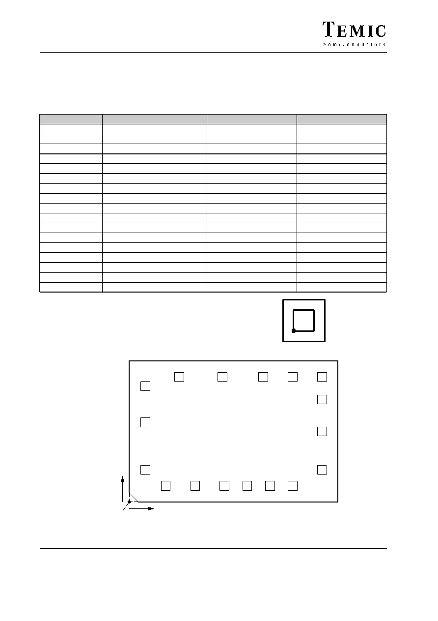
PAD Coordinates
The T4225B is only available as die for “chip-on-board” mounting.
DIE size:
2.26 x 1.54 mm
PAD size:
100 x 100
mm (contact window 88 x 88 mm)
Thickness:
300
mm " 20 mm
Symbol
Function
x-axis/
mm
y-axis/
mm
IN1
Amplifier input (inverted)
128
846
IN
Amplifier input (non inverted)
128
310
GND
Ground
354
124
SB
Bandwidth control
696
128
Q1A
Crystal filter 1
1040
128
Q1B
Crystal filter 1
1290
128
REC
Rectifier output
1528
128
INT
Integrator output
1766
128
DEC
Decoder input
2044
268
FLA
Lowpass filter
2044
676
FLB
Lowpass filter
2044
1072
SL
AGC hold mode
2044
1310
Q2A
Crystal filter 2
1724
1324
Q2B
Crystal filter 2
1402
1324
PON
Power-ON/OFF control
918
1324
TCO
Time-code output
460
1324
VCC
Supply voltage
128
1246
The PAD coordinates are referred to the left bottom point
of the contact window.
PAD Layout
VCC
TCO
PON
Q2B
Q2A
SL
FLB
FLA
DEC
INT
REC
Q1B
Q1A
SB
GND
IN
IN1
Reference point (%)
x – axis
y – axis
T4225B
95 10386
Figure 2.
發(fā)布緊急采購,3分鐘左右您將得到回復。