- 您現在的位置:買賣IC網 > PDF目錄385880 > SW-437PIN GaAs SPDT Switch DC - 3.0 GHz PDF資料下載
參數資料
| 型號: | SW-437PIN |
| 英文描述: | GaAs SPDT Switch DC - 3.0 GHz |
| 中文描述: | 砷化鎵單刀雙擲開關直流- 3.0吉赫 |
| 文件頁數: | 1/3頁 |
| 文件大?。?/td> | 94K |
| 代理商: | SW-437PIN |
GaAs SPD Switch, DC - 3.0 GHz
SW-437
SW-437
M/A-COM Division of AMP Incorporated North America: Tel. (800) 366-2266, Fax (800) 618-8883 Asia/Pacific: Tel.+81 44 844 8296, Fax +81 44 844 8298
Europe: Tel. +44 (1344) 869 595, Fax+44 (1344) 300 020
www.macom.com
AMP and Connecting at a Higher Level are trademarks.
Specifications subject to change without notice.
V2.00
GaAs SPDT Switch
DC - 3.0 GHz
Features
Low Cost Plastic SOT-363 Package
Low Insertion Loss <0.3dB @ 900 MHz
Low Power Consumption <15μA @ +2.7V
Positive or Negative 2.5 to 8 V Control
Description
M/A-COM’s SW-437 is a GaAs monolithic switch in a low cost
SOT-363 surface mount plastic package. The SW-437 is ideally
suited for applications where very low power consumption, low
insertion loss, very small size and low cost are required. Typical
application is in dual band systems where switching between
small signal components is required such as filter banks, single
band LNA's, converters etc. The SW-437 can be used in applica-
tions up to 0.25 Watts in systems such as cellular, PCS,
DCS1800, GSM, CDMA, W-CDMA and other analog/digital
wireless communications systems.
The SW-437 is fabricated using a mature 0.8 micron GaAs
MESFET process. The process features full passivation for
increased performance and reliability.
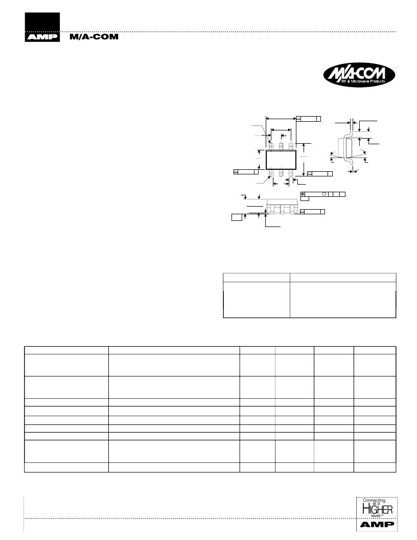
SOT-363 Plastic Package
1
Electrical Specifications T
A
= 25°C
Ordering Information
Part Number
SW-437 PIN
SW-437TR
SW-437RTR
SW-437SMB
Package
SOT-363 Plastic Package
Forward Tape and Reel
1
Reverse Tape and Reel
1
Sample Board
1. Reference Application Note M513 for reel size information.
Parameter
Test Conditions
Units
dB
dB
dB
dB
dB
dB
Min.
Typ.
0.3
0.4
0.55
21
15
12
1.2:1
24
27
81
55
10
20
10
4
Max.
0.4
0.5
0.7
Insertion Loss
DC - 1 GHz
1- 2 GHz
2 - 3 GHz
DC - 1 GHz
1 - 2 GHz
2 - 3 GHz
DC - 3 GHz
500 MHz - 3 GHz
500 MHz - 3 GHz
2-Tone 900 MHz, 5 MHz spacing (2.7 V)
2-Tone 900 MHz, 5 MHz spacing (2.7 V)
10% to 90% RF, 90% to 10% RF
50% Control to 90% RF, Control to 10% RF
In-Band
V
CTL
= 2.5 V
Isolation
19
13
10
VSWR
P
1dB
(2.7V supply)
P
1dB
(5V supply)
Input IP
2
Input IP
3
T
rise
,
T
fall
T
,
T
T
ransients
Gate Leakage
1.3:1
dBm
dBm
dBm
dBm
ns
ns
mV
μA
15
1. All dimensions are JEDEC MO-203-AB Issue A and are shown
as in/mm.
.0059 (0.15) C
2X
.0079 (0.20) C
2X
.0059 (0.15) C
2X
.0039 (0.10) C
2X
.0492
1,25
.0256
0,65
.0512
1,3
.0787
2
.0827
2,1
PIN 6
-D-
.0098
.0031
0,25
0,08
.0142
±
.0039
0,30
±
0,1
.0165
0,42
REF
10
°
4
°
8
°
0
°
10
°
4
°
.0118
.0059
0,30
0,15
-A-
.0039 (0.10) M
B
C
A
B D
PIN 1
+.0038
-.0079
+0,10
-0,20
.0354
0,90
.0433
1,10
MAX
-C-
.0039
.0000
0,10
0,00
##X
相關PDF資料 |
PDF描述 |
|---|---|
| SW-437RTR | GaAs SPDT Switch DC - 3.0 GHz |
| SW-437TR | GaAs SPDT Switch DC - 3.0 GHz |
| SW-438TR-3000 | GaAs SPDT Switch DC. 3.0 GHz |
| SW-438 | GaAs SPDT Switch DC. 3.0 GHz |
| SW-438SMB | GaAs SPDT Switch DC. 3.0 GHz |
相關代理商/技術參數 |
參數描述 |
|---|---|
| SW-437RTR | 制造商:MA-COM 制造商全稱:M/A-COM Technology Solutions, Inc. 功能描述:GaAs SPDT Switch DC - 3.0 GHz |
| SW-437SMB | 制造商:MA-COM 制造商全稱:M/A-COM Technology Solutions, Inc. 功能描述:GaAs SPDT Switch DC - 3.0 GHz |
| SW-437TR | 制造商:M/A-COM Technology Solutions 功能描述:0 MHz - 3000 MHz RF/MICROWAVE SGL POLE DOUBLE THROW SWITCH, 0.7 dB INSERTION LOSS |
| SW-437TR-3000 | 制造商:M/A-COM Technology Solutions 功能描述: |
| SW-438 | 制造商:MA-COM 制造商全稱:M/A-COM Technology Solutions, Inc. 功能描述:GaAs SPDT Switch DC. 3.0 GHz |
發(fā)布緊急采購,3分鐘左右您將得到回復。