- 您現(xiàn)在的位置:買賣IC網(wǎng) > PDF目錄372313 > ST901T (意法半導(dǎo)體) HIGH VOLTAGE IGNITION COIL DRIVER NPN POWER DARLINGTON PDF資料下載
參數(shù)資料
| 型號(hào): | ST901T |
| 廠商: | 意法半導(dǎo)體 |
| 英文描述: | HIGH VOLTAGE IGNITION COIL DRIVER NPN POWER DARLINGTON |
| 中文描述: | 高壓點(diǎn)火線圈驅(qū)動(dòng)達(dá)林頓NPN電源 |
| 文件頁數(shù): | 135/199頁 |
| 文件大?。?/td> | 2813K |
| 代理商: | ST901T |
第1頁第2頁第3頁第4頁第5頁第6頁第7頁第8頁第9頁第10頁第11頁第12頁第13頁第14頁第15頁第16頁第17頁第18頁第19頁第20頁第21頁第22頁第23頁第24頁第25頁第26頁第27頁第28頁第29頁第30頁第31頁第32頁第33頁第34頁第35頁第36頁第37頁第38頁第39頁第40頁第41頁第42頁第43頁第44頁第45頁第46頁第47頁第48頁第49頁第50頁第51頁第52頁第53頁第54頁第55頁第56頁第57頁第58頁第59頁第60頁第61頁第62頁第63頁第64頁第65頁第66頁第67頁第68頁第69頁第70頁第71頁第72頁第73頁第74頁第75頁第76頁第77頁第78頁第79頁第80頁第81頁第82頁第83頁第84頁第85頁第86頁第87頁第88頁第89頁第90頁第91頁第92頁第93頁第94頁第95頁第96頁第97頁第98頁第99頁第100頁第101頁第102頁第103頁第104頁第105頁第106頁第107頁第108頁第109頁第110頁第111頁第112頁第113頁第114頁第115頁第116頁第117頁第118頁第119頁第120頁第121頁第122頁第123頁第124頁第125頁第126頁第127頁第128頁第129頁第130頁第131頁第132頁第133頁第134頁當(dāng)前第135頁第136頁第137頁第138頁第139頁第140頁第141頁第142頁第143頁第144頁第145頁第146頁第147頁第148頁第149頁第150頁第151頁第152頁第153頁第154頁第155頁第156頁第157頁第158頁第159頁第160頁第161頁第162頁第163頁第164頁第165頁第166頁第167頁第168頁第169頁第170頁第171頁第172頁第173頁第174頁第175頁第176頁第177頁第178頁第179頁第180頁第181頁第182頁第183頁第184頁第185頁第186頁第187頁第188頁第189頁第190頁第191頁第192頁第193頁第194頁第195頁第196頁第197頁第198頁第199頁
135/199
ST90158 - SERIAL PERIPHERAL INTERFACE (SPI)
SERIAL PERIPHERAL INTERFACE
(Cont’d)
9.5.3 Functional Description
The SPI, when enabled, receives input data from
the internal data bus to the SPI Data Register
(SPIDR). A Serial Clock (SCK) is generated by
controlling through software two bits in the SPI
Control Register (SPICR). The data is parallel
loaded into the 8 bit shift register during a write cy-
cle. This is shifted out serially via the SDO pin,
MSB first, to the slave device, which responds by
sending its data to the master device via the SDI
pin. This implies full duplex transmission if 3 I/O
pins are used with both the data-out and data-in
synchronized with the same clock signal, SCK.
Thus the transmitted byte is replaced by the re-
ceived byte, eliminating the need for separate “Tx
empty” and “Rx full” status bits.
When the shift register is loaded, data is parallel
transferred to the read buffer and becomes availa-
ble to the CPU during a subsequent read cycle.
The SPI requires three I/O port pins:
SCK
Serial Clock signal
SDO
Serial Data Out
SDI
Serial Data In
An additional I/O port output bit may be used as a
slave chip select signal. Data and Clock pins I2C
Bus protocol are open-drain to allow arbitration
and multiplexing.
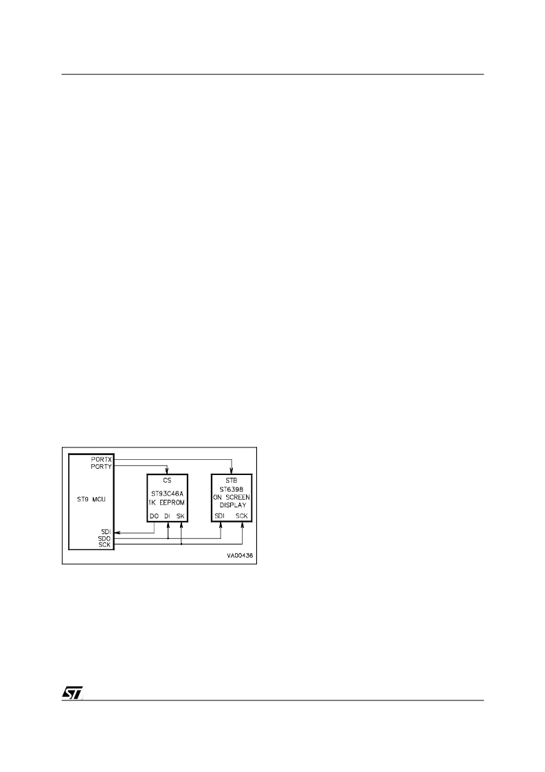
Figure 66
below shows a typical SPI network.
Figure 66. A Typical SPI Network
n
9.5.3.1 Input Signal Description
Serial Data In (SDI)
Data is transferred serially from a slave to a mas-
ter on this line, most significant bit first. In an S-
BUS/I
2
C-bus configuration, the SDI line senses
the value forced on the data line (by SDO or by an-
other peripheral connected to the S-bus/I
2
C-bus).
9.5.3.2 Output Signal Description
Serial Data Out (SDO)
The SDO pin is configured as an output for the
master device. This is obtained by programming
the corresponding I/O pin as an output alternate
function. Data is transferred serially from a master
to a slave on SDO, most significant bit first. The
master device always allows data to be applied on
the SDO line one half cycle before the clock edge,
in order to latch the data for the slave device. The
SDO pin is forced to high impedance when the SPI
is disabled.
During an S-Bus or I
2
C-Bus protocol, when arbi-
tration is lost, SDO is set to one (thus not driving
the line, as SDO is configured as an open drain).
Master Serial Clock (SCK)
The master device uses SCK to latch the incoming
data on the SDI line. This pin is forced to a high im-
pedance state when SPI is disabled (SPEN,
SPICR.7 = “0”), in order to avoid clock contention
from different masters in a multi-master system.
The master device generates the SCK clock from
INTCLK. The SCK clock is used to synchronize
data transfer, both in to and out of the device,
through its SDI and SDO pins. The SCK clock
type, and its relationship with data is controlled by
the CPOL (Clock Polarity) and CPHA (Clock
Phase) bits in the Serial Peripheral Control Regis-
ter (SPICR). This input is provided with a digital fil-
ter which eliminates spikes lasting less than one
INTCLK period.
Two bits, SPR1 and SPR0, in the Serial Peripheral
Control Register (SPICR), select the clock rate.
Four frequencies can be selected, two in the high
frequency range (mostly used with the SPI proto-
col) and two in the medium frequency range
(mostly used with more complex protocols).
9
相關(guān)PDF資料 |
PDF描述 |
|---|---|
| ST9291J7B1 | Microcontroller |
| ST9291N2B1 | Microcontroller |
| ST9291N3B1 | Microcontroller |
| ST9291N4B1 | Microcontroller |
| ST9291N5B1 | Microcontroller |
相關(guān)代理商/技術(shù)參數(shù) |
參數(shù)描述 |
|---|---|
| ST901T_05 | 制造商:STMICROELECTRONICS 制造商全稱:STMicroelectronics 功能描述:HIGH VOLTAGE IGNITION COIL DRIVER NPN POWER TRANSISTOR |
| ST901TFP | 功能描述:兩極晶體管 - BJT PWR BIP/S.SIGNAL RoHS:否 制造商:STMicroelectronics 配置: 晶體管極性:PNP 集電極—基極電壓 VCBO: 集電極—發(fā)射極最大電壓 VCEO:- 40 V 發(fā)射極 - 基極電壓 VEBO:- 6 V 集電極—射極飽和電壓: 最大直流電集電極電流: 增益帶寬產(chǎn)品fT: 直流集電極/Base Gain hfe Min:100 A 最大工作溫度: 安裝風(fēng)格:SMD/SMT 封裝 / 箱體:PowerFLAT 2 x 2 |
| ST9020B1 | 制造商:未知廠家 制造商全稱:未知廠家 功能描述:8-Bit Microcontroller |
| ST9020B6 | 制造商:未知廠家 制造商全稱:未知廠家 功能描述:8-Bit Microcontroller |
| ST9027 | 制造商:STMICROELECTRONICS 制造商全稱:STMicroelectronics 功能描述:16K PROM / 256 RAM HCMOS MCUS |
發(fā)布緊急采購,3分鐘左右您將得到回復(fù)。