- 您現(xiàn)在的位置:買(mǎi)賣(mài)IC網(wǎng) > PDF目錄372313 > ST90158M7T6 8-BIT MICROCONTROLLER PDF資料下載
參數(shù)資料
| 型號(hào): | ST90158M7T6 |
| 元件分類: | 8位微控制器 |
| 英文描述: | 8-BIT MICROCONTROLLER |
| 中文描述: | 8位微控制器 |
| 文件頁(yè)數(shù): | 93/199頁(yè) |
| 文件大?。?/td> | 2813K |
| 代理商: | ST90158M7T6 |
第1頁(yè)第2頁(yè)第3頁(yè)第4頁(yè)第5頁(yè)第6頁(yè)第7頁(yè)第8頁(yè)第9頁(yè)第10頁(yè)第11頁(yè)第12頁(yè)第13頁(yè)第14頁(yè)第15頁(yè)第16頁(yè)第17頁(yè)第18頁(yè)第19頁(yè)第20頁(yè)第21頁(yè)第22頁(yè)第23頁(yè)第24頁(yè)第25頁(yè)第26頁(yè)第27頁(yè)第28頁(yè)第29頁(yè)第30頁(yè)第31頁(yè)第32頁(yè)第33頁(yè)第34頁(yè)第35頁(yè)第36頁(yè)第37頁(yè)第38頁(yè)第39頁(yè)第40頁(yè)第41頁(yè)第42頁(yè)第43頁(yè)第44頁(yè)第45頁(yè)第46頁(yè)第47頁(yè)第48頁(yè)第49頁(yè)第50頁(yè)第51頁(yè)第52頁(yè)第53頁(yè)第54頁(yè)第55頁(yè)第56頁(yè)第57頁(yè)第58頁(yè)第59頁(yè)第60頁(yè)第61頁(yè)第62頁(yè)第63頁(yè)第64頁(yè)第65頁(yè)第66頁(yè)第67頁(yè)第68頁(yè)第69頁(yè)第70頁(yè)第71頁(yè)第72頁(yè)第73頁(yè)第74頁(yè)第75頁(yè)第76頁(yè)第77頁(yè)第78頁(yè)第79頁(yè)第80頁(yè)第81頁(yè)第82頁(yè)第83頁(yè)第84頁(yè)第85頁(yè)第86頁(yè)第87頁(yè)第88頁(yè)第89頁(yè)第90頁(yè)第91頁(yè)第92頁(yè)當(dāng)前第93頁(yè)第94頁(yè)第95頁(yè)第96頁(yè)第97頁(yè)第98頁(yè)第99頁(yè)第100頁(yè)第101頁(yè)第102頁(yè)第103頁(yè)第104頁(yè)第105頁(yè)第106頁(yè)第107頁(yè)第108頁(yè)第109頁(yè)第110頁(yè)第111頁(yè)第112頁(yè)第113頁(yè)第114頁(yè)第115頁(yè)第116頁(yè)第117頁(yè)第118頁(yè)第119頁(yè)第120頁(yè)第121頁(yè)第122頁(yè)第123頁(yè)第124頁(yè)第125頁(yè)第126頁(yè)第127頁(yè)第128頁(yè)第129頁(yè)第130頁(yè)第131頁(yè)第132頁(yè)第133頁(yè)第134頁(yè)第135頁(yè)第136頁(yè)第137頁(yè)第138頁(yè)第139頁(yè)第140頁(yè)第141頁(yè)第142頁(yè)第143頁(yè)第144頁(yè)第145頁(yè)第146頁(yè)第147頁(yè)第148頁(yè)第149頁(yè)第150頁(yè)第151頁(yè)第152頁(yè)第153頁(yè)第154頁(yè)第155頁(yè)第156頁(yè)第157頁(yè)第158頁(yè)第159頁(yè)第160頁(yè)第161頁(yè)第162頁(yè)第163頁(yè)第164頁(yè)第165頁(yè)第166頁(yè)第167頁(yè)第168頁(yè)第169頁(yè)第170頁(yè)第171頁(yè)第172頁(yè)第173頁(yè)第174頁(yè)第175頁(yè)第176頁(yè)第177頁(yè)第178頁(yè)第179頁(yè)第180頁(yè)第181頁(yè)第182頁(yè)第183頁(yè)第184頁(yè)第185頁(yè)第186頁(yè)第187頁(yè)第188頁(yè)第189頁(yè)第190頁(yè)第191頁(yè)第192頁(yè)第193頁(yè)第194頁(yè)第195頁(yè)第196頁(yè)第197頁(yè)第198頁(yè)第199頁(yè)
93/199
ST90158 - I/O PORTS
INPUT/OUTPUT BIT CONFIGURATION
(Cont’d)
When Px.n is programmed as an Output
:
(
Figure 52
)
– The Output Buffer is turned on in an Open-drain
or Push-pull configuration.
– The data stored in the Output Master Latch is
copied both into the Input Latch and into the Out-
put Slave Latch, driving the I/O pin, at the end of
the execution of the instruction.
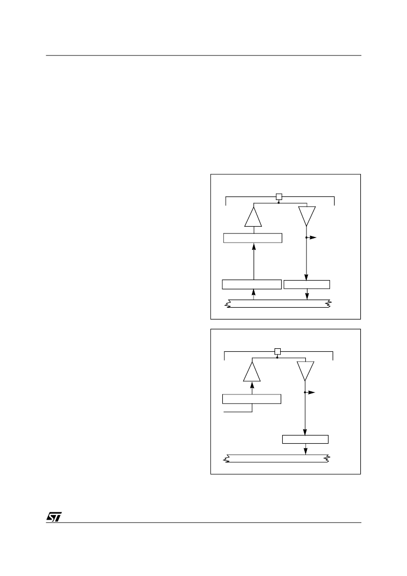
When Px.n is programmed as Bidirectional
:
(
Figure 53
)
– The Output Buffer is turned on in an Open-Drain
or Weak Pull-up configuration (except when dis-
abled in hardware).
– The data present on the I/O pin is sampled into
the Input Latch at the beginning of the execution
of the instruction.
– The data stored in the Output Master Latch is
copied into the Output Slave Latch, driving the I/
O pin, at the end of the execution of the instruc-
tion.
WARNING
: Due to the fact that in bidirectional
mode the external pin is read instead of the output
latch, particular care must be taken with arithme-
tic/logic and Boolean instructions performed on a
bidirectional port pin.
These instructions use a read-modify-write se-
quence, and the result written in the port register
depends on the logical level present on the exter-
nal pin.
This may bring unwanted modifications to the port
output register content.
For example:
Port register content, 0Fh
external port value, 03h
(Bits 3 and 2 are externally forced to 0)
A
bset
instruction on bit 7 will return:
Port register content, 83h
external port value, 83h
(Bits 3 and 2 have been cleared).
To avoid this situation, it is suggested that all oper-
ations on a port, using at least one bit in bidirec-
tional mode, are performed on a copy of the port
register, then transferring the result with a load in-
struction to the I/O port.
When Px.n is programmed as a digital Alter-
nate Function Output
:
(
Figure 54
)
– The Output Buffer is turned on in an Open-Drain
or Push-Pull configuration.
– The data present on the I/O pin is sampled into
the Input Latch at the beginning of the execution
of the instruction.
– The signal from an on-chip function is allowed to
load the Output Slave Latch driving the I/O pin.
Signal timing is under control of the alternate
function. If no alternate function is connected to
Px.n, the I/O pin is driven to a high level when in
Push-Pull configuration, and to a high imped-
ance state when in open drain configuration.
Figure 53. Bidirectional Configuration
n
n
Figure 54. Alternate Function Configuration
n
n
n
n
n
n
OUTPUT MASTER LATCH
INPUT LATCH
OUTPUT SLAVE LATCH
INTERNAL DATA BUS
I/O PIN
WEAK PULL-UP
OPEN DRAIN
TTL
(or Schmitt Trigger)
TO PERIPHERAL
INPUTS AND
INTERRUPTS
INPUT LATCH
FROM
PERIPHERAL
OUTPUT
INTERNAL DATA BUS
I/O PIN
OPEN DRAIN
PUSH-PULL
TTL
(or Schmitt Trigger)
TO PERIPHERAL
INPUTS AND
INTERRUPTS
OUTPUT SLAVE LATCH
9
相關(guān)PDF資料 |
PDF描述 |
|---|---|
| ST90158M9 | 8/16-BIT MICROCONTROLLER (MCU) WITH 16 TO 64K ROM. OTP OR EPROM. 512 TO 2K RAM - ST9 + FAMILY |
| ST90158M9LVT6 | 8/16-BIT MICROCONTROLLER (MCU) WITH 16 TO 64K ROM. OTP OR EPROM. 512 TO 2K RAM - ST9 + FAMILY |
| ST90158M9T6 | 8-BIT MICROCONTROLLER |
| ST90R158M9LVT6 | FUSE,5A,250V,5X20MM,FAST ACTING |
| ST90R158T6 | 8/16-BIT MICROCONTROLLER (MCU) WITH 16 TO 64K ROM. OTP OR EPROM. 512 TO 2K RAM - ST9 + FAMILY |
相關(guān)代理商/技術(shù)參數(shù) |
參數(shù)描述 |
|---|---|
| ST90158M9 | 制造商:未知廠家 制造商全稱:未知廠家 功能描述:8/16-BIT MICROCONTROLLER (MCU) WITH 16 TO 64K ROM. OTP OR EPROM. 512 TO 2K RAM - ST9 + FAMILY |
| ST90158M9LVT6 | 制造商:未知廠家 制造商全稱:未知廠家 功能描述:8/16-BIT MICROCONTROLLER (MCU) WITH 16 TO 64K ROM. OTP OR EPROM. 512 TO 2K RAM - ST9 + FAMILY |
| ST90158M9Q6 | 制造商:STMICROELECTRONICS 制造商全稱:STMicroelectronics 功能描述:8/16-BIT MCU FAMILY WITH UP TO 64K ROM/OTP/EPROM AND UP TO 2K RAM |
| ST90158M9T1 | 制造商:STMICROELECTRONICS 制造商全稱:STMicroelectronics 功能描述:8/16-BIT MCU FAMILY WITH UP TO 64K ROM/OTP/EPROM AND UP TO 2K RAM |
| ST90158M9T6 | 制造商:未知廠家 制造商全稱:未知廠家 功能描述:8-Bit Microcontroller |
發(fā)布緊急采購(gòu),3分鐘左右您將得到回復(fù)。
