- 您現(xiàn)在的位置:買賣IC網(wǎng) > PDF目錄385870 > ST6395B1 (意法半導體) 8-BIT HCMOS MCUs FOR TV FREQUENCY SYNTHESIS WITH OSD PDF資料下載
參數(shù)資料
| 型號: | ST6395B1 |
| 廠商: | 意法半導體 |
| 英文描述: | 8-BIT HCMOS MCUs FOR TV FREQUENCY SYNTHESIS WITH OSD |
| 中文描述: | 8位微控制器HCMOS電視頻率合成帶OSD |
| 文件頁數(shù): | 13/68頁 |
| 文件大小: | 560K |
| 代理商: | ST6395B1 |
第1頁第2頁第3頁第4頁第5頁第6頁第7頁第8頁第9頁第10頁第11頁第12頁當前第13頁第14頁第15頁第16頁第17頁第18頁第19頁第20頁第21頁第22頁第23頁第24頁第25頁第26頁第27頁第28頁第29頁第30頁第31頁第32頁第33頁第34頁第35頁第36頁第37頁第38頁第39頁第40頁第41頁第42頁第43頁第44頁第45頁第46頁第47頁第48頁第49頁第50頁第51頁第52頁第53頁第54頁第55頁第56頁第57頁第58頁第59頁第60頁第61頁第62頁第63頁第64頁第65頁第66頁第67頁第68頁
ST639x CORE
(Continued)
Stack
The ST639x Core includes true LIFO hardware
stack that eliminates the need for a stack pointer.
The stackconsists of six separate 12-bit RAM lo-
cations that do not belong to the data space RAM
area. When a subroutine call (or interruptrequest)
occurs,the contentsofeachlevelis shiftedinto the
next levelwhile the contentof the PCis shiftedinto
the first level (the value of the sixth level will be
lost). When subroutine or interrupt return occurs
(RET orRETI instructions),thefirst levelregisteris
shifted backintothe PCand thevalueof eachlevel
is shifted back into the previous level. These two
operating modes are described in Figure 7. Since
the accumulator,as all otherdata space registers,
is notstored inthisstack thehandlingof thisregis-
ters shall be performed inside the subroutine. The
stack pointer will remain in its deepest position, if
more than 6 calls or interrupts are executed, so
that the last return address will be lost. It will also
remain in its highest position if the stack is empty
and a RET or RETI is executed. In this case the
next instruction will be executed.
Memory Registers
The PRPR
can be addressed like a RAM location
in the Data Space at the CAh address; neverthe-
less it is a write-only register that can not be ac-
cessed with single-bit operations.This register is
used to select the 2-Kbyte ROM bank of the Pro-
gram Spacethat will be addressed.The numberof
the page hastobe loaded inthePRPR. ThePRPR
is not cleared during the MCU initialization and
should therefore be definedbefore jumping out of
the static page. Refer to the Program Space de-
scription for additional information concerning the
use of this register. The PRPR is not modified
when an interrupt or a subroutine occurs.
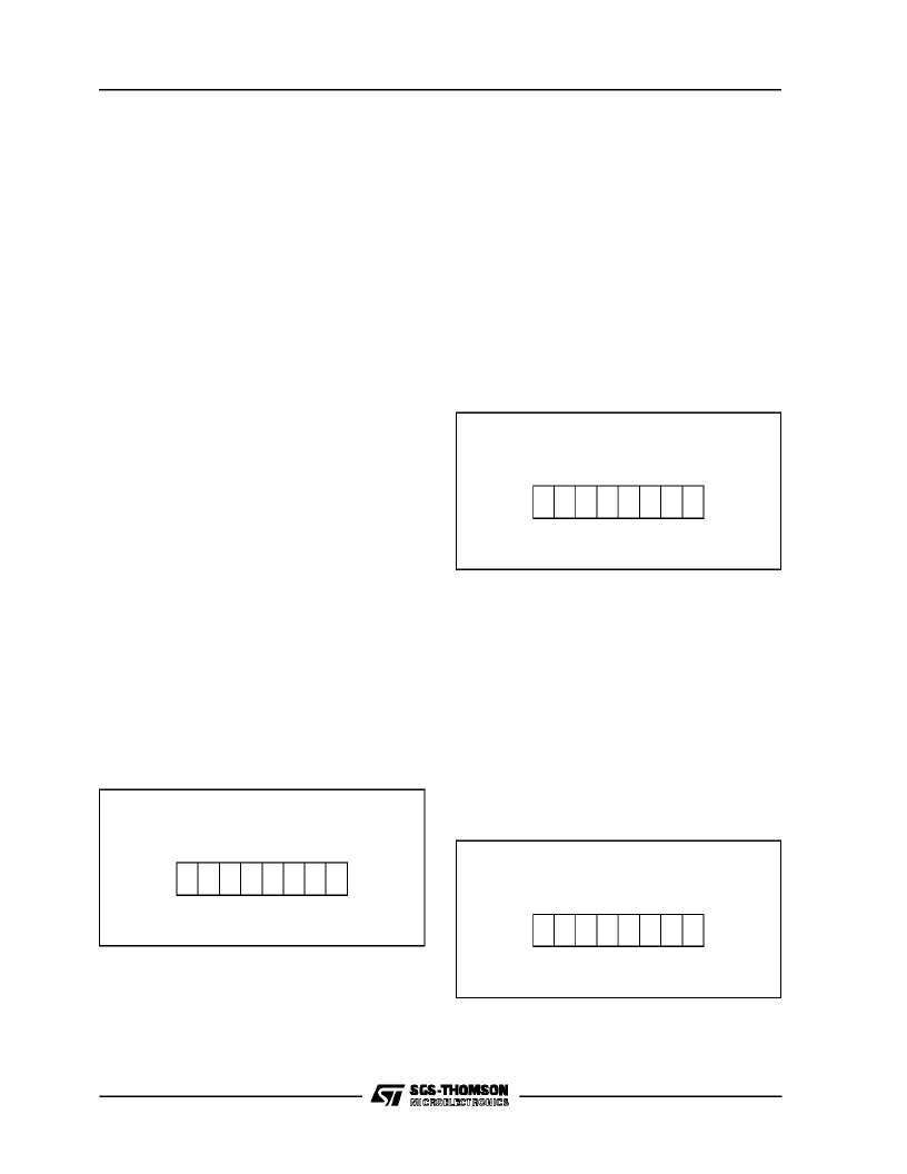
PRPR
Program ROMPage Register
(CAh, Write Only)
D7 D6 D5 D4 D3 D2 D1 D0
Figure8. Program ROMPage Register
DRBR
Data RAM Bank Register
(E8h, Write Only)
D7 D6 D5 D4 D3 D2 D1 D0
Figure 9. Data RAM Bank Register
DRWR
Data ROM Window Register
(C9h, Write Only)
D7 D6 D5 D4 D3 D2 D1 D0
Figure 10. Data ROM Window Register
The DRBR
can be addressedlike a RAMlocation
in the Data Space at the E8h address, neverthe-
less it is write-only register that can not be ac-
cessed with single-bit operations. This register is
used to select the desired 64-byteRAM/EEPROM
bank of the Data Space. The number of the bank
has to be loaded in the DRBR and the instruction
has to point tothe selected locationasit was in the
0 bank (from 00h address to 3Fh address). This
register isundefined afterReset. Refer to the Data
Space description for additional information. The
DRBRregisteris not modifiedwhena interruptor a
subroutine occurs.
TheDRWR
registercanbeaddressedlikeaRAMlo-
cationin theDataSpaceat the C9h address,never-
theless it is write-only register that can not be
accessed with single-bit operations.This register is
used to move up and down the 64-byte read-only
datawindow (from the40h addressto 7Fh address
of the Data Space) along the ROM of the MCU by
stepof 64bytes.The effectiveaddressof thebyteto
bereadasadatainthe ROMisobtainedbythecon-
catenationofthe6lesssignificantbitsoftheaddress
given in the instruction (as less significant bits) and
the contentof the DRWR (as most significantbits).
Referto the DataSpacedescriptionforadditionalin-
formation.
ST6391,92,93,95,97,99
9/64
相關(guān)PDF資料 |
PDF描述 |
|---|---|
| ST6391B1 | MOSFET; Transistor Polarity:Dual N Channel; Continuous Drain Current, Id:2.6A; On-Resistance, Rds(on):0.18ohm; Package/Case:8-SOIC; Leaded Process Compatible:No; Mounting Type:surface mount; Peak Reflow Compatible (260 C):No |
| ST6392 | 8-BIT HCMOS MCUs FOR TV FREQUENCY SYNTHESIS WITH OSD |
| ST6393 | 8-BIT HCMOS MCUs FOR TV FREQUENCY SYNTHESIS WITH OSD |
| ST6395 | 8-BIT HCMOS MCUs FOR TV FREQUENCY SYNTHESIS WITH OSD |
| ST6397 | 8-BIT HCMOS MCUs FOR TV FREQUENCY SYNTHESIS WITH OSD |
相關(guān)代理商/技術(shù)參數(shù) |
參數(shù)描述 |
|---|---|
| ST6397 | 制造商:STMICROELECTRONICS 制造商全稱:STMicroelectronics 功能描述:8-BIT HCMOS MCUs FOR TV FREQUENCY SYNTHESIS WITH OSD |
| ST6397B1 | 制造商:STMICROELECTRONICS 制造商全稱:STMicroelectronics 功能描述:8-BIT HCMOS MCUs FOR TV FREQUENCY SYNTHESIS WITH OSD |
| ST6399 | 制造商:STMICROELECTRONICS 制造商全稱:STMicroelectronics 功能描述:8-BIT HCMOS MCUs FOR TV FREQUENCY SYNTHESIS WITH OSD |
| ST6399B1 | 制造商:STMICROELECTRONICS 制造商全稱:STMicroelectronics 功能描述:8-BIT HCMOS MCUs FOR TV FREQUENCY SYNTHESIS WITH OSD |
| ST63E126D1 | 制造商:STMICROELECTRONICS 制造商全稱:STMicroelectronics 功能描述:8-BIT HCMOS MCUs FOR TV FREQUENCY & VOLTAGE SYNTHESIS WITH OSD |
發(fā)布緊急采購,3分鐘左右您將得到回復。