- 您現(xiàn)在的位置:買賣IC網(wǎng) > PDF目錄385866 > ST24LC21M1TR (意法半導(dǎo)體) Pulse Width Modulation (PWM) Controller IC; Topology:Push Pull; Control Mode:Current; Number of PWM Outputs:1; Input Voltage Primary Min:10V; Input Voltage Primary Max:120V; Duty Cycle Max:50%; Oscillator Frequency Max, Fosc:1MHz PDF資料下載
參數(shù)資料
| 型號: | ST24LC21M1TR |
| 廠商: | 意法半導(dǎo)體 |
| 英文描述: | Pulse Width Modulation (PWM) Controller IC; Topology:Push Pull; Control Mode:Current; Number of PWM Outputs:1; Input Voltage Primary Min:10V; Input Voltage Primary Max:120V; Duty Cycle Max:50%; Oscillator Frequency Max, Fosc:1MHz |
| 中文描述: | 1kB的x8串行EEPROM的雙模式為韋莎插頭 |
| 文件頁數(shù): | 5/18頁 |
| 文件大小: | 149K |
| 代理商: | ST24LC21M1TR |
AI01665
VCC
CBUS
SDA
RL
MASTER
RL
SCL
CBUS
100
0
4
8
12
16
20
CBUS (pF)
M
)
10
1000
fc = 400kHz
fc = 100kHz
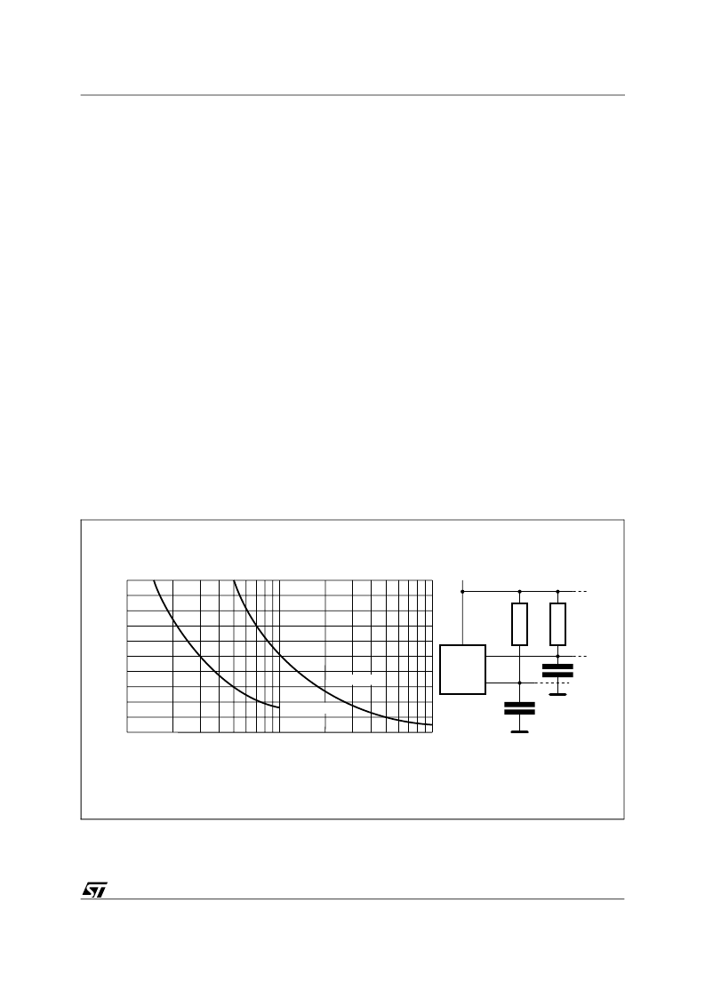
Figure 5. Maximum R
L
Value versus Bus Capacitance (C
BUS
) for an I
2
C Bus
SIGNAL DESCRIPTIONS
I
2
C Serial Clock (SCL).
The SCL input pin is used
to synchronize all data in and out of the memory. A
resistor can be connected from the SCL line to V
CC
to act as a pull up (see Figure 5).
Transmit Only Clock (VCLK).
The VCLK input pin
is used to synchronize data out when the
ST24LC21 is in Transmit Only mode. The VCLK
input offers also a Write Enable (active high) func-
tion when the ST24LC21 is in I
2
C bidirectional
mode.
Serial Data (SDA).
The SDA pin is bi-directional
and is used to transfer data in or out of the memory.
It is an open drain output that may be wire-OR’ed
with other open drain or open collector signals on
the bus. A resistor must be connected from the SDA
bus line to V
CC
to act as pull up (see Figure 5).
DEVICE OPERATION
I
2
C Bus Background
The ST24LC21 supports the I
2
C protocol. This
protocol defines any device that sends data onto
the bus as a transmitter and any device that reads
the data as a receiver. The device that controls the
data transfer is known as the master and the other
as the slave. The master will always initiate a data
transfer and will provide the serial clock for syn-
chronisation. The ST24LC21 are always slave de-
vices in all communications.
Start Condition.
START is identified by a high to
low transition of the SDA line while the clock SCL
is stable in the high state. A START condition must
precede any command for data transfer. Except
during a programming cycle, the ST24LC21 con-
tinuously monitor the SDA and SCL signals for a
START condition and will not respond unless one
is given.
Stop Condition.
STOP is identified by a low to high
transition of the SDA line while the clock SCL is
stable in the high state. A STOP condition termi-
nates communication between the ST24LC21 and
the bus master. A STOP condition at the end of a
Read command forces the standby state. A STOP
condition at the end of a Write command triggers
the internal EEPROM write cycle.
Acknowledge Bit (ACK).
An acknowledge signal
is used to indicate a successfull data transfer. The
bus transmitter, either master or slave, will release
the SDA bus after sending 8 bits of data. During the
9th clock pulse period the receiver pulls the SDA
bus low to acknowledge the receipt of the 8 bits of
data.
5/18
ST24LC21
相關(guān)PDF資料 |
PDF描述 |
|---|---|
| ST2600C | MOSFET, N, SO-8; Transistor type:MOSFET; Current, Id cont:13.4A; Resistance, Rds on:0.009R; Voltage, Vgs Rds on measurement:4.5V; Case style:SO-8 PowerPak; Charge, gate n-channel:50nC; Current, Idm pulse:50A; Depth, external:5.26mm; RoHS Compliant: Yes |
| ST280S04P1V | PHASE CONTROL THYRISTORS Stud Version |
| ST280S06P1V | PHASE CONTROL THYRISTORS Stud Version |
| ST280S | PHASE CONTROL THYRISTORS Stud Version |
| ST300S12M1L | PHASE CONTROL THYRISTORS |
相關(guān)代理商/技術(shù)參數(shù) |
參數(shù)描述 |
|---|---|
| ST24LW21 | 制造商:STMICROELECTRONICS 制造商全稱:STMicroelectronics 功能描述:1 Kbit x8 Dual Mode Serial EEPROM for VESA PLUG & PLAY |
| ST24LW21B1 | 制造商:未知廠家 制造商全稱:未知廠家 功能描述:I2C Serial EEPROM |
| ST24LW21B1TR | 制造商:STMICROELECTRONICS 制造商全稱:STMicroelectronics 功能描述:1 Kbit x8 Dual Mode Serial EEPROM for VESA PLUG & PLAY |
| ST24LW21B6 | 制造商:未知廠家 制造商全稱:未知廠家 功能描述:I2C Serial EEPROM |
| ST24LW21B6TR | 制造商:STMICROELECTRONICS 制造商全稱:STMicroelectronics 功能描述:1 Kbit x8 Dual Mode Serial EEPROM for VESA PLUG & PLAY |
發(fā)布緊急采購,3分鐘左右您將得到回復(fù)。